Designing custom PCB Layout for your complex electronics projects often comes with challenges. A simple mistake, no matter how minor it looks, will make your project malfunction. These common mistakes in PCB design right from the very beginning will also increase custom PCB manufacturing costs.
This article would explain 15 common mistakes that you should know and avoid when designing a custom PCB. Don’t worry, even if you are a newcomer, as even experienced engineers can also make these mistakes. Avoiding them will mean a high-quality product, reduced custom PCB production cost, no fabrication delays, and no rework requirements. So, let’s get started.
Contents
- 1 Not Considering the Available PCB Design Tools
- 2 Narrow High-Current Traces
- 3 Inappropriate Placement of Decoupling Capacitors
- 4 No Optimization of Switching Regulators Layout
- 5 Mistakes when Drawing Landing Patterns
- 6 Non-manufacturable Buried or Blind Vias
- 7 Improper Antenna Layouts
- 8 Long High-speed Traces
- 9 Not Getting a Second Opinion
- 10 Large Slithers
- 11 Complex Custom PCB Designs
- 12 Utilizing Incorrect Components or Custom PCB Layout Methods
- 13 Custom PCB Layout–Forgetting to Save All the PCB Design Files
- 14 Not Consulting Custom PCB Manufacturers Early
- 15 Custom PCB Layout– No Testing of Custom PCB
- 16 Summary
Not Considering the Available PCB Design Tools
Designers don’t usually consider all the available and easy-to-use custom PCB design tools. That is a critical mistake as many design tools are there for fulfilling various needs and flexibility requirements of PCBs. You can use custom PCB design software for tasks such as scanning design errors, component placement, and prototype development. This software is quite cheap, web-based, or even freely accessible.
Narrow High-Current Traces
Narrow widths of PCB traces would not be enough if your project must deal with current more significant than a few hundred milliamps. Keep in mind that the external layer PCB trace can carry current higher than the internal layer’s evidence of the same thickness. The reason being the former has more heat dissipation and airflow.
Many custom PCB manufacturers will give you options to select from copper weights ranging from 0.5 oz/sqft to 2.5 oz/sqft. We would recommend you use a trace width calculator for calculating its current-carrying capability.
Inappropriate Placement of Decoupling Capacitors
Decoupling capacitors in a custom PCB design serve those pins which require a stable and clean voltage. You may place them close to the pins for sufficient, calm energy. Further, the power trace of the power supply rail also connects to the bolt via the decoupling capacitor. You can also place an inductor in series to make a Low-pass filter for removing any input noise.
No Optimization of Switching Regulators Layout
In electronic custom PCB designs, voltage regulators are of two types: linear and switching regulators. Linear regulators are easy to layout, cheap but can waste loads of electric power. However, switching regulators, although complex, are quite efficient as they spend very little energy. You will get a longer battery life with them. So, it is critical to follow the datasheet guidelines while making their PCB layout.
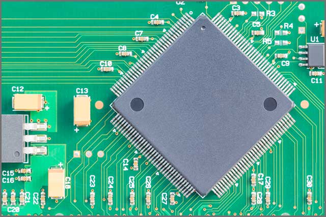
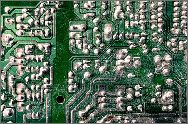
Mistakes when Drawing Landing Patterns
Software for custom PCB design supplies libraries for components that comprise their PCB landing pattern and schematic symbol. There will not be any problems if you only use the library components. But you will need to manually draw the landing pattern and schematic symbol of a part that is not already there. Therefore, you need to be careful because even if the pad-to-pad spacing deviates only by a millimeter, there will be soldering and alignment problems.
Non-manufacturable Buried or Blind Vias
We would recommend that you not use blind or buried vias for PCB prototyping if you are on a budget. The through vias go through all the layers of PCB, and they surely increase the PCB size. However, they are inexpensive as compared to buried or blind vias. An embedded system makes an electrical connection with two internal layers, and a blind via connects an internal and external layer.
It is worth mentioning that it is not as easy as it sounds. You need to maintain the design constraints related to layer stacking when designing the custom PCB layout.
Improper Antenna Layouts
Antenna custom PCB layouts are very crucial for electronic projects employing wireless tech. Even the electrical engineers sometimes draw it incorrectly. You may need to match the complex impedance of the antenna and transceiver for maximum power transmission. So, for that purpose, a proper transmission line is required.
For most antennas, a transmission line with a 50-ohm impedance is enough for max power transmission. You can find out the transmission line’s proportions by using free online calculators such as AppCAD. You can also put an LC pi-network between the transceiver and the antenna for fine-tuning the antenna impedance.
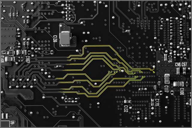
Long High-speed Traces
Signals with high-speed should adopt the straightest and shortest available path. It would help if you directed any high-frequency crystals while designing the custom PCB properly. Many PCB designs based on microcontrollers only need a few high-speed signals. Still, if your project has a microprocessor with high-speed, an address bus, and external data, then you need to be watchful.

Not Getting a Second Opinion
Engineers are often working under a tight deadline and absorbed in getting the result for custom PCB production. Results in custom PCB design errors. Therefore, it is best to get your PCB design reviewed by another engineer to avoid high costs in the later custom PCB production stages. The rule is simple: mistakes become more expensive if you detect them in later stages.
Large Slithers
Slithers are copper lumps that remain undissolved during the chemical etching process. It can seem that these adhere to the PCB and the customized PCB manufacturing appearance, which will also cause short circuits. Thus, it would help if you made sure that the minimum width of copper is more than the requirement of a custom PCB manufacturer. In this way, slithers will diminish, and your PCB will work properly.
Complex Custom PCB Designs
Custom PCB manufacturers can produce PCBs more efficiently and economically if they know their fundamental working. But, if the design is sophisticated, it can create problems such as an imbalanced schematic. Therefore, you must try your best to simplify your custom PCB designs to avoid any design errors. Also, this will increase the effectiveness of your design.

Utilizing Incorrect Components or Custom PCB Layout Methods
The need of the hour is to design complex custom PCB layouts using smaller components and reduced footprints. For such purposes, designers are using ball grid array packages and embedded devices on PCB’s inner layers. It helps in advancing the project performance and allowing rework if there are any errors.
You must select the correct layout method for components with smaller pitch and higher pin count. Doing this in the design stage will save your custom PCB production costs. Moreover, if you plan to use a substitute component, be sure to check that its performance characteristics match the original so that you do not need to throw away the custom PCB design in the later stages.
Custom PCB Layout–Forgetting to Save All the PCB Design Files
Always back up your custom PCB design files. The files can get lost if your software starts not to respond, so don’t wait to save them until the whole design is complete. You should at least store the files that are hard to get back. Most custom PCB manufacturers provide daily backups, but smaller firms may not offer such facilities. Also, this will not be possible if you are working individually from your home.
With the advent of “Cloud” services these days, no excuse is there to safely back up the PCB design files. If you plan to do mass production of your product or want to release it into the market, this will also ensure that your custom PCB design is safe from fire, forgery, threat, malware, and other tech disasters.

Not Consulting Custom PCB Manufacturers Early
Custom PCB manufacturers usually follow their registered production processes that increase the efficiency of their staff and equipment. If you do not take care of their manufacturing methods, your project cost can rise or manufacturing delays. You will also be wasting your time as you will need to contact another custom PCB manufacturer. Also, you may need to redesign the custom PCB layout according to the manufacturer’s specifications.

Custom PCB Layout– No Testing of Custom PCB
Once you have made the custom PCB prototypes, you should inspect it thoroughly. It should be made sure that the initial operational requirements of the design are fulfilling. Further, you may also test the environmental conditions that can affect the stability or reliability of PCB. That is to ensure a wide-range operation of your custom PCB. If you don’t do that, your custom PCB prototype can fail when it finally releases into the market.
Summary
Therefore, there are 15 custom PCB design problems that you need to pay special attention to avoid. We can assure you that you can mostly prevent fabrication problems that may occur if you do so. We, WellPCB, will also carefully review your designs when they are received. You can contact us today if you need any help. So, what are you waiting for?


