Contents
What is HDI PCB?
In today’s face-paced industry, circuit board Making. THE conventional PCB routing methods can not achieve this. With HDI PCBs offer companies and designers a chance to double the circuit while reducing the area. The acronym ‘fabrication of rigid PCBs. Here, the conditions apply to multilayer, single-sided, metalcore, HDI‘ stands for High-Density Interconnector. These HDI Printed Circuit Boards or HDI PCBs are regular circuit boards that feature a higher density of wires throughout the surface area.
That results in a drastic reduction in the size and weight of the equipment. Not only that, but it enhances the electrical performance of the equipment. Furthermore, it allows for faster and more efficient transmission of data due to the shortening of the paths.
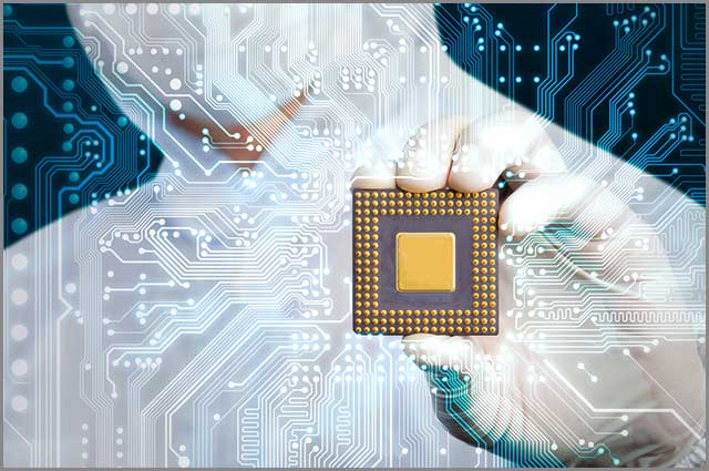
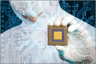
Image 1: HDI PCB
You can easily distinguish them through the micro-vias, more delicate lines, thin materials as well as a higher pad density. These micro-vias may be blind or buried and up to about 0.006 in diameter. Thus, you can say that the HDI PCB has given birth to the miniaturization of products.
Microvias and HDI PCBs
Before we move on to designing HDI PCBs, you must learn the role of micro vias in HDI PCBs. Micro vias are fine holes drilled by a laser that links two different layers electrically in a multi-layer circuit board.
Unlike vias, they are much smaller in size and are thus directly related to the miniaturization and space-saving qualities of HDI PCBs.
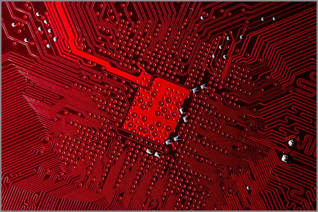
Image 2: HDI PCB
HDI Structures
Usually, HDI PCBs can be designed in many ways. These are:
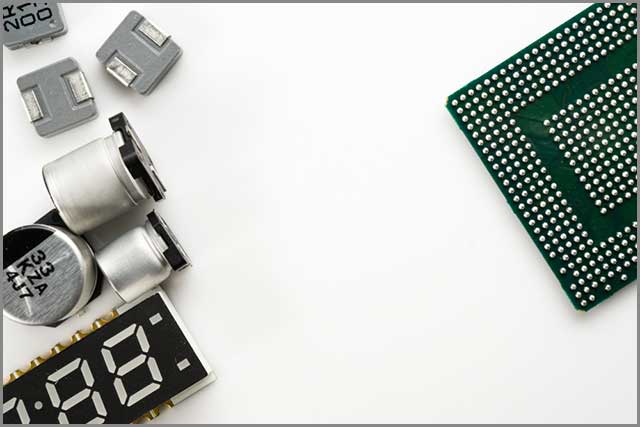
Image 3: HDI PCB
1+N+1:
It indicates there is only a single high-density interconnection layer in PCBs.
i+N+i:
It indicates that there are two or more than 2 HDI layers in PCBs. Moreover, the micro-vias are either stacked or staggered together on the different layers.
Any layers:
In this structure, all the layers are HDI layers, which enable the interconnectivity of all the layers. It proves to be beneficial for complex devices such as GPU chips on smartphones or CPU chips on the computer.
HDI Design Rules and Tips
Generally, PCB designing is an intricate task. Couple that with micro vias and HDI circuits, and you have got yourself a complicated mess. The complications are further intensified when aerospace systems and medical devices are involved.
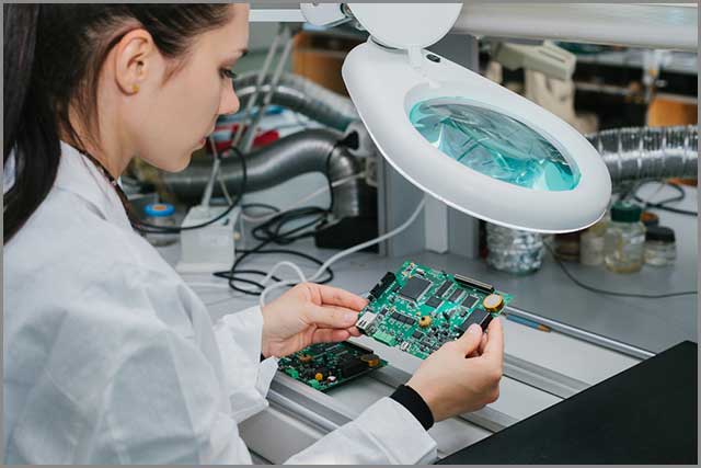
Image 4: HDI PCB
Adopt a DFM Strategy
Our first tip is pretty simple and general. It is essential that incorporate a DFM or Design manufacturing strategy with HDI PCBs. If you end up designing something that is far beyond the capabilities of your contract manufacturer (CM) then, the design might be useless.
You must design the board to provide all the benefits of the HDI PCB and be easily manufactured at the same time.
Choose the Type of Via
Choosing via type is a crucial decision that determines the machine and equipment you might need in the manufacturing process. It can heavily influence the costs involved in the process as well as the time.
Micro vias, in itself, reduce manufacturing time and costs by reducing the number of layers and materials. However, you have to choose between the different types. These include the near pad or the via in-pad versions.
Thus, you must choose one that costs you or your CM the least to manufacture without compromising the electrical performance of the HDI PCB.
Check Availability and Size of the Components
Another point to consider is the number of components you hope to use for HDI PCB. Remember that the number one objective of the HDI PCB is to reduce the costs and surface area. You need to ensure that they are small, inexpensive, and as less in number as possible.
Moreover, the way you place your components can determine the size of holes, trace widths, and backups. However, wne should consider the availability and functionality of these components. Otherwise, you could end up redesigning the entire board.
Do Not Overcrowd Components
While the compact design might force your hand towards placing components close together, you should probably avoid it. High-power components, especially, can give rise to Electromagnetic interference (EMI), which can affect the quality of the signal.
Also, capacitances and inductances from pads close by can affect the signal quality and delay transmission. So, wne recommend that you provide sufficient space between components.
Also, ensure that all components are placed to distribute the vias symmetrically across the surface. It reduces the stress, which in turn prevents any warping.
Generally, the spacing between the components should be:
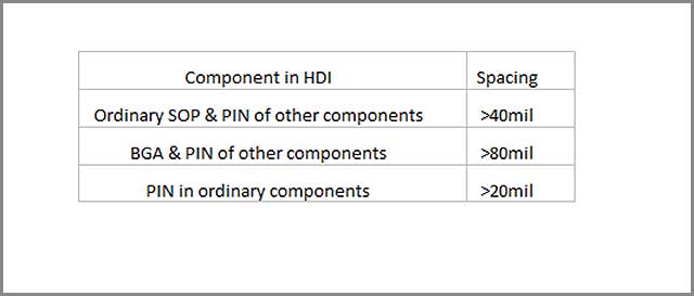
Image 5: HDI PCB
Consider the installation and maintenance as well, so the components are easy to solder and rework later. If they’re too close to each other, the machines might have trouble assembling them.
Choose a Stackup Design
The type of PCB stack-up can also determine any complications in the manufacturing process. The number of laminates and the drilling cycles are heavily affected by the kind of materials and the number of layers in the stack design. Ensure that whatever you choose is effective yet cost-friendly.
HDI PCB Prototype
An HDI Prototype is a basic version of an HDI PCB that you can use to test out various designs. You can either ask your CM to manufacture these prototypes for you. These prototypes consist of high-density wiring that helps reduce the size as well as the number of layers.
These prototypes should utilize staggered, stacked, buried, and blind vias so you can determine which combination works best. Also, the prototype can help you choose the size of the vias and the most efficient aspect ratio.
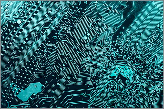
Image 6: HDI PCB

Advantages of HDI PCB
There are numerous benefits that an HDI PCB offers.
Less Thermal Stress
Because the components are closer together in an HDI PCB, the heat doesn’t travel a lot. The shorter distances between the members ensure that the heat is quickly expelled before transferring to the other components.
It ensures lesser thermal stress and adds to the durability of the PCB.
Better Conductivity
The HDI PCB helps in ensuring better conductivity due to a large number of micro vias. These are filled with conductive materials that allow for easier transmission. Furthermore, these vias, whether they are blind or via-in-pad ones, allow components to be placed very close to each other.
That, in turn, reduces the transmission range between the two components, and thus, it significantly boosts the signal.
Allows for Miniaturization
As HDI PCBs help significantly reduce the space on the board, they can help you design smaller circuit boards. Not only this, but it enables you to reduce the number of layers as you can create circuits on both sides of the board. Thus, it is easy to replace the four-layer PCB with a two-layer PCB.
Also, the vias are so delicate and minute. They are barely visible. It helps in saving a ton of space. Thus, this ensures that you can make smaller circuit boards that can fit in a smaller device.
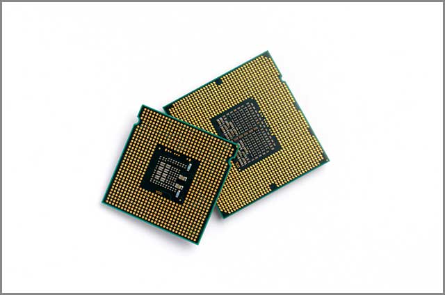
Image 7: HDI PCB
The Decrease in Power Usage
Transmission from one component to the next can lose a lot of energy. Luckily, HDI PCBs allow you to incorporate more elements with fewer distances. That reduces energy losses and uses more energy in actual operation.
Furthermore, it leads to a longer battery life, which is quite desirable in handheld and other smaller devices.
Cost-Effective
A significant advantage of the HDI PCB technology is that these circuits are relatively cost-effective if appropriately designed. This is due to the fewer layers and the smaller sizes.
Faster Yield
Since the main focus is on optimizing the design to reduce costs and ensure higher throughput, the product is more comfortable to place all components, ensuring that the process takes less time and enters the market much quicker. We assure you that’s enough to find out about the advantages of HDI PCB.
HDI PCB Stackup
As we already mentioned, HDIs consist of multiple layers interconnected by microvias. They work together to form connections and boost the signal. How you arrange these HDI layers in a PCB defines the type of HDI PCB Stackup. You can catch a glimpse of the more specific types above in our HDI PCB design section.
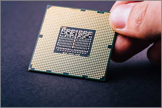
Image 8: HDI PCB
Generally, there are various types of HDI PCB stack-ups, some of which are:
0-N-0 – Laser Microvia
In this, the manufacturer laminates the core first and then mechanically drills it. Then, the mechanical drill gets plated and is hit with a laser to form vias. Lastly, they include the final through the hole.
1-N-1 – Laser Microvia& Buried Via
The ‘1’ stands for the sequential lamination that occurs on both sides of the core. It means that there are two HDI layers on either side of the body. The process is similar to the above one, except that after the mechanical drill gets plated, an internal layer is formed.
This core layer is then laminated by two additional layers so that the mechanical drill acts as a buried via. Next, a laser drill forms more vias.
2-N-2 with Microvia
The ‘2’ here represents two layers of lamination on either side of the core. Thus, you can say that there are four copper layers, so there are a total of 6 layers in this type.
HDI PCB Capability
The HDI PCB is capable of supporting innovation and small products. It is because it can easily incorporate more technology into fewer layers. Mobiles and smartphones have started a trend of slimmer and lighter products, which is only possible due to this breakthrough PCB technology.
Thus, you get products that weigh less and perform more functions while being extremely small in size. It not only makes the products more comfortable to use but also easier to manufacture. They make use of thinner and lighter materials that are easier to manufacture.
All in all, you get a four-layered HDI PCB, which has the same wiring solder mask to prevent leakage of electrical and thermal components. Be sure to discuss with your PCB supplier about the capabilities as that of an eight-layer standard PCB. It might even perform more functions due to closer components, making more space for additions.
You might ask if it is more expensive to manufacture through micro or HDI. Well, yes, it requires an intricate design as well as laser drills, laser imaging, plugging, etc., to fabricate a proper HDI PCB. However, the minor components, cheaper materials, and processes effectively reduce the prices of these products. So, you get an amazingly innovative product at a lesser price.
With the discovery of better technology every day, HDI PCBs are used in many ways. These are:
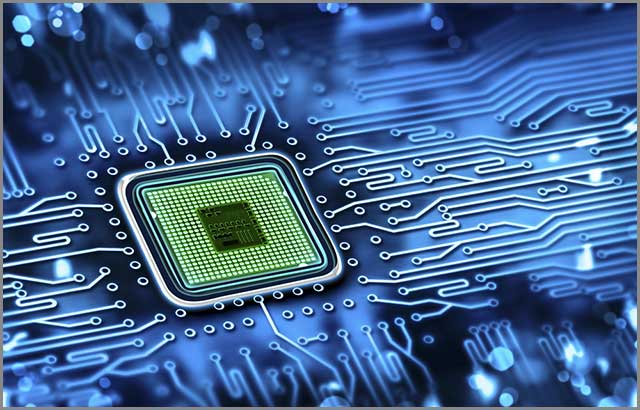
Image 9: HDI PCB
Medical Equipment
The technical features and functionality of diagnostic and monitoring equipment have seen a hike with the HDI PCBs. It ensures better reliability, which is crucial in the field of medicine.
Military
HDI PCBs find their use in military communication devices as well as other equipment.
Computers and Smartphones
GPU and CPU chips use HDI PCBs to enhance their performance and ensure a smaller size and lighter weight.
Aerospace Industry
The Aerospace industry heavily benefits from these smaller and lighter chips.
HDI PCBs offer an excellent chance for manufacturers to maximize their profits. However, there are various factors you need to consider about HDI PCB Assemblies, which we’ll discuss in our next chapter.
The Emergence of Cheap PCB
The Assembly of HDI PCBs involves a variety of unique processes that utilize special equipment. These can include sequential lamination cycles as well as high laser drills. Thus, if your manufacturing company or CM doesn’t have this equipment included, it could increase an added investment.
The total cost of the HDI PCB will change as the stack-up height changes. Also, designers need to consider the value of the materials of the components, including the filling inside the vias.
The material of each core layer and the number of layers also affect the cost. Amongst these, fiberglass is the most functional and inexpensive. These layers can determine the number of copper lamination layers the board will have. The more layers, the higher, will be the cost.
Another factor that you need to consider when assembling the product is a minimum trace space. The main takeaway is that while manufacturing and making HDI PCBs can be expensive, the costs can be minimized in the design process.
So, designers and electronic engineers need to ensure that their design corresponds with the CM’s capabilities. The HDI PCB can be ultimately cheaper than standard PCBs, depending on the design and the materials used.
Image 10: HDI PCB
Conclusion
All in all, HDI PCBs result in better yields and ensure ideal performance. However, finding a manufacturer who can provide you with reliable services can be difficult. It is where we at WellPCB come in. Our manufacturing capabilities are comprehensive, and so we can easily manufacture prototypes according to your designs.
Our reliability tests determine the quality of all the products to ensure satisfactory service. So, head on over to our website and get your quote now!


