Contents
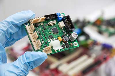
What Are Printed Circuit Boards?
Printed circuit boards are essentially substrated circuitry. They offer a more organized and cleaner way to facilitate the transmission of electric currents. PCBs achieve this through a combination of metal traces and etched electric components. Printed circuit boards are available in a wide variety of layers, sizes and types.
PCBs are an essential part of modern technology. It’s quite difficult to find any sufficiently complex machinery or electronics that do not use a PCB of some sort.
Abstract Technology Chip Processor Background Circuit Stock Vector
Where Are Printed Circuit Boards Used?
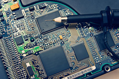
Electronics manufacturers and inventors have integrated PCBs into devices since the 1960s. Today, you can find them in almost any electronic device you use. They’re in your LCD-based computer screen, motherboard, personal computer motherboard, smart-phone, etc. Essentially, printed circuit boards are the foundation of modern electronic devices.
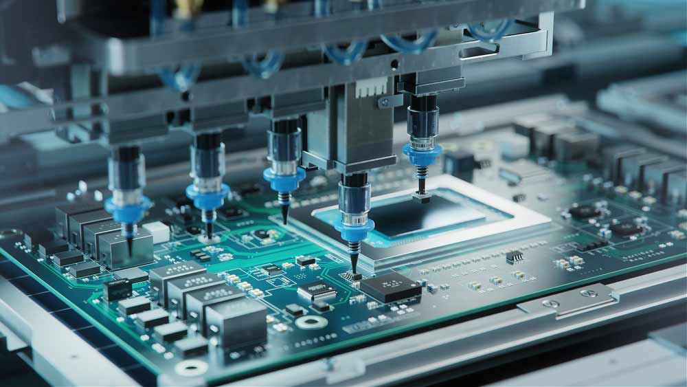
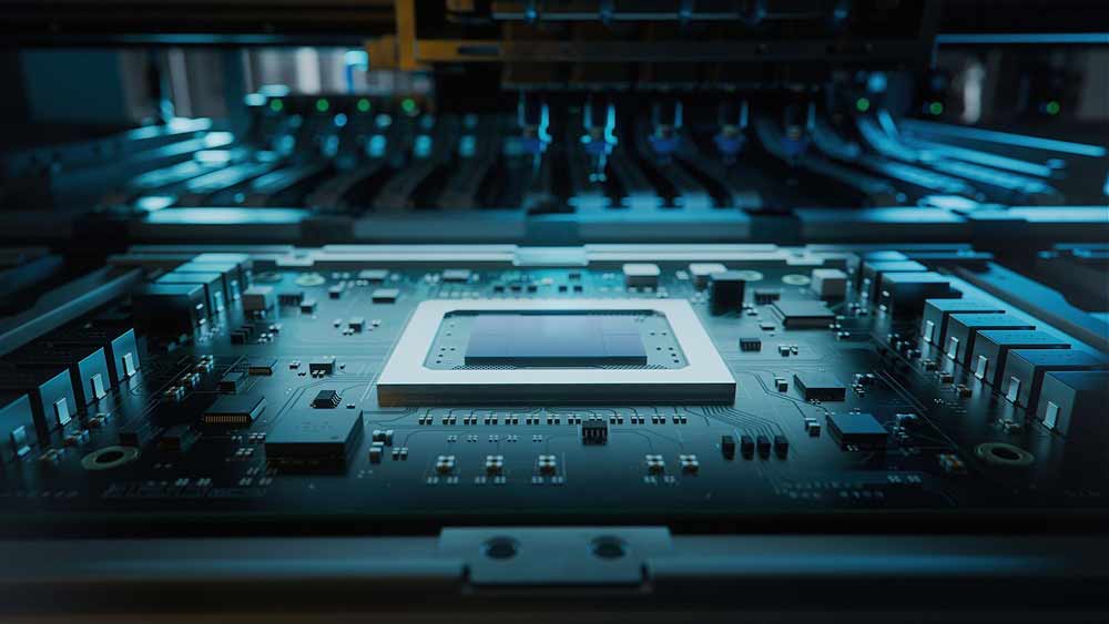
Automatic Pick Place Machine Quickly Installs
The PCB is one of the greatest inventions in history. The history of PCB traces back to over 130 years.
Interestingly, the industrial machine has advanced throughout with adjustments and enhancements. As a result, it’s almost impossible to compare the first PCBs with modern designs.
But as the famous saying goes: “You need to know where it starts to know where it’s headed.” Hence, we’ll take you through where it all started, the idea behind the device, the inventors, and more.
Are you ready? Let’s get the ball rolling.
The History of PCBs
Albert Hanson, a German scientist, was one of the individuals who started a quest to create a more straightforward electrical pathway. His invention didn’t look like PCBs, but it paved the way for the device’s creation.
Albert filed a patent for a device in 1903 to enhance telephone exchange boards.
Indeed, the device was a bare circuit board that featured wires bonded to a flat surface with conductive pieces.
Albert’s circuit board had a through-hole construction with conductors but lacked modern precursors.
In 1927, Charles Ducas, an American inventor, took a bold step forward in the PCB world. And he started by printing wires directly on a board with a stencil. Then, he added ink to conduct electricity. The goal of the invention was to place an electronic path on an insulated surface. Interestingly, Ducas came up with a device that looked like a printed circuit board.
Even though Ducas figured out the circuit board, he contemplated the possibility of having a multilayered circuit board by connecting many boards. Hence, it took another great mind to see Ducas’ ideas and bring them to light.
And the man that dotted the I’s and crossed the T’s was Paul Eisler. Hence, it’s no surprise that he gets a lot of credit for inventing the PCB.
But it all happened when he settled in England after leaving Austria. The Austrian Inventor had a background in the printing industry, so it helped birth the idea of printing electronic circuits on boards.
And his creation eased the labor-intensive practice of hand-soldering wires to your boards. Further, one of his PCBs had its first application in radio—which Americans and British found resourceful during World War II.
Evolution Timeline Of PCB
1925
An American inventor, Charles Ducas, drew conductive materials on a wooden plane board. And it was a patent for his first circuit board design.
1936
Paul Eisler, an Austrian inventor, created the first PCB. And it was helpful in a radio set.
1943
Paul went a step further by patenting a more advanced PCB design. The design required etching the circuits against copper foil on a non-conductive substrate.
1944
Britain and America joined forces to create proximity fuse in artillery shells, mines, and bombs during WWII.
1948
There was an overall development of the PCB technology as the U.S Army released it to the public.
The 1950s
Transistors hit the electronics market. Consequently, it reduced the size of electronics. Hence, it was easier to add PCBs—which enhanced the reliability of electronics.
The 1950s – 1960s
PCBs advanced into boards (double-sided) with printing identification on one side and electrical components on the other. Also, PCB designs had zinc plates, coatings, and corrosion-resistant materials to avoid deterioration.
The 1960s
Electronic designs had silicon chips or integrated circuits. Hence, it became possible to have a single chip with tens of thousands of components. Consequently, there was a significant improvement in electronics’ reliability, power, and speed.
Also, the PCB had more layers to contain the new IC’s conductors. But since the IC chips were small, PCBs reduced in size, and soldering connections became challenging.
The 1970s
There was a mix-up between the printed circuit boards and polychlorinated biphenyl (an environmentally harmful chemical) because both of them had the PCB abbreviation at that time. As a result, there were community health concerns and public confusion.
Hence, the device’s scientists changed the name to PWB (printed wiring board) to reduce confusion. This name remained until the 1990s, when chemical PCBs phased out.
The 1970s – 1980s
To ease the solder application of copper circuits, solder masks were developed of thin polymer materials. And this helped to bridge adjacent courses and boost circuit density.
After a while, inventors developed a photo imageable polymer coating. With this, engineers could apply the layer directly to the circuits, desiccate, and modify by photo exposure. And this further enhanced circuit density. Hence, it became the PCB standard manufacturing method.
The 1980’s
Surface-mount technology (SMT) came into play as a new assembly technology. Initially, all PCB components featured wire leads. Hence, it was vital to solder the components into the PCB holes. The holes took up a lot of space, which was useful for extra circuit routing.
So, SMT components became the manufacturing standard. And engineers soldered the components to small pads on the PCB without using the holes. Over time, SMT components replaced through-hole parts and became the industry standard.
As a result, reliability, performance, and functional power increased. And there was a reduction in production costs.
The 1990s
There was a continuous reduction in PCB size due to CAM/CAD (computer-aided manufacturing and design) software prominence. Also, mechanical designs contributed to the automation of PCB design.
Further, it helps to ease increasingly complex designs with lighter and smaller parts. In addition, more minor connections permit fast-increasing PCB shrinking or miniaturization.
The 2000s
PCBs tick the boxes for increased complexity, compatibility, higher layer counts, and lightness. That said, the flexible circuit and multilayered PCB design permit increased operational functionality in electronic devices with smaller and cheaper PCBs.

Printed Circuit Boards Today
These days, there’s no confusion associated with PCBs. Because we have outlived the era of chemical PCBs, no doubt, in the industry, you can use the terms PWB (printed wire board) and printed circuit board interchangeably. But the more familiar word is printed circuit board.
The latest innovation that has hit PCB technology is the rigid-flex PCB. Interestingly, this technology combines a hardboard circuit with a rigid structure and complexity.
So, thanks to the combined layers, the rigid-flex PCBs are thinner, smaller, and can fit into small or unusually shaped products.
What Does the Future Hold For PCBs?
Due to recent technological advancements, engineers can print circuit boards with multi-step procedures like photolithographic and conventional vacuum deposition patterning.
That sounds good, right? True, but it’s hard to ignore the snags associated with this level of technology. The PCBs are pricey, require a high processing temperature, and involve toxic waste.
And with all that’s going on in this industry, the PCBs will revolutionize soon. After all, it has already started as 3d printing is becoming a thing. Hence, 3D printing PCBs is a reality.
Furthermore, research institutes have predicted the future of PCBs to be green. So, we should expect paper-printed circuit boards.
Also, the drive-by manufacturers to produce smaller electronic appliances will move PCB production design to smaller boards with higher capacities.
Plus, we should expect to see more 3D molded plastic boards, embedded components, integrated chips, and POP (package on package) becoming a thing.
These advancements are undoubtedly the forerunners that will keep the PCB industry constantly growing—as the years move.
FAQs
When did PCBs first come out?
PCBs first came out in 1936, after Paul Eisler, an Austrian inventor, developed one to use in a radio system. Paul Eisler used Charle’s Ducas galvanic plating of copper to design the PCB.
What is the history of PCB etching?
You can trace the roots of PCB etching back to 1913 when English inventor Arthur Berry first patented the print-and-etch method. This method illustrated how you can create circuits that have metal etched away from them.
He also described how you could coat the metal in a protective layer of resistance before etching. This was an improvement over other methods, such as cutting, which left etch fractures with sharp corners.
Other methods that are in the same vein of PCB etching include John Sargroves Electronic Circuit Making Equipment (ECME), which existed from 1936 to 1947.
It sprayed metal onto a Bakelite plastic board. Advancements into etching continued into the 20th century with radio equipment manufacturer Hallicrafters releasing one of the the first photo-etched PCBs in its 1952 clock radio.
Over the years, various entities, inventors, and organizations, such as the US Army, continued developing the PCB assembly and fabrication process. Etching and lamentation techniques also improved, ultimately leading to the techniques and processes we have today.
Shot Generic Printed Circuit Board Microchips
Why are some PCBs black?
PCBs get their color from the solder mask. Manufacturers apply solder masks to protect copper traces from oxidation (rust) and prevent solder bridges from forming.
The solder masks come in a variety of colors – with green seemingly being the most favored among manufacturers.
Black is another option.
Manufacturers may produce black PCBs for niche electronic products that stand out. For instance, certain computer motherboard manufacturers use different-colored PCBs for their product lines.
Their high-end gaming motherboards may be black, while their low—to mid-range products may be green.
Nevertheless, the color has no real bearing on the quality or capabilities of the PCB.
Rounding Up
WellPCB has been in the business of PCB fabrication for years. We always deliver on our promise of providing the industry’s best quality PCBs. Plus, we use the latest PCB technology.
Furthermore, our rigid-flex PCBs can be complex and time-consuming to fabricate. But we handle all the flexible parts carefully. Then, we pass the printed circuit board through quality assurance testing and surpass industry standards.
In addition, we have brand new equipment and an overall production area of 10,000 m2. Hence, we can deliver over 10,000 varieties and 30,000 m2 feet of 2-32-layer PCBs monthly.
So, do you need to get the best PCBs for your projects? Please feel free to contact us.