
Contents
1. PCB Production—Stages Of PCB Production
The schematic design is error-free, with proper connections and supplies.
Components placed for the PCB layout have a correct footprint, drilling size of pads, and proper orientation.
The routing is appropriate between the right parts with relevant trace width.
Cross-checking every detail, along with their reference designator and nets, and design rules check often.
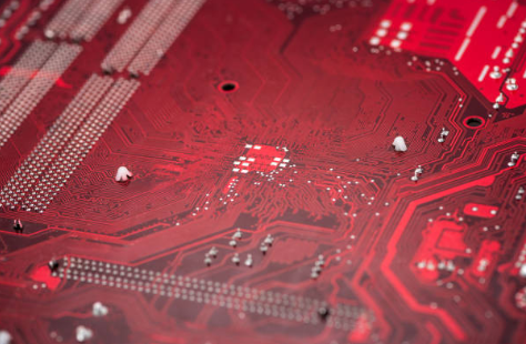
Now comes the PCB production phase.
For this, it is advisable to first develop a PCB prototype before going for total production.
This gives designers to test their circuit and the actual layout in physical form, and then once satisfied, they can order the total output of that PCB.
The main stages of PCB Production are:
Step 1: Selecting PCB material
The popular PCB substrate materials belong to the FR series, among which the most common is FR4. FR4 material-based PCB is a glass, fiber-based board.
It is yellowish-green and offers good mechanical and reasonable stability under various temperatures.
The best part is that it is not excessively expensive. Other materials, such as FR2, FR3, FR-5, CEM1, CEM3, and PTFE, are available at low costs.
The copper-clad board is obtained to make a printed circuit board.
This is done by a copper cladding that bonds a thin layer of copper on both sides of the substrate.
Step 2: Tracking on PCB
The next step is creating tracks onboard. A photographic process is used to gain the correct channels on the board.
The photophotoresistrial covers the copper on the PCB, which is then exposed to light through a photomask or a photographic film.
These details required tracks onto the photophotoresistic.
After completing this process, the photophotoresistlaced in a developer to cover that area where ways are needed.
Step 3: Etching PCB
The next stage involves etching those areas where copper isn’t required.
This is usually done by a chemical etching process, most commonly using a ferric chloride solution.
The board is placed in the etching agent for a certain amount of time, according to the concentration of the ferric chloride solution and the thickness of the copper.
Step 4: Creating vias and holes
Small holes or vias are created in complex PCBs to ensure electrical connection between different layers. There are three types of vias: blind, buried, and through-hole.
Furthermore, holes may need to be added to the PCB to mount leaded components. For these holes, drilling is done using drill files from the Gerber files.
The drill file data is supplied to PCB CAD design software which controls drilling machines to make holes. Make sure that the sizes of the holes are not much different.
The fewer the number of different hole sizes, the cheaper the PCB cost.
Step 5: Solder plating of PCB
To protect areas on the PCB that don’t need to be soldered, a polymer layer called solder resist is applied to them.
In addition, this deep green or red layer also prevents short circuits that can cause by solder during soldering and from contamination.
The mounting areas are platted or tinned with solder for soldering leaded components or mounting SMT components.
Occasionally, these exposed areas may be gold-plated.
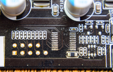
Step 6: PCB SilkScreen
Often, the text is printed on PCB for marking components or identifying the board.
For this, PCB design software generates a silkscreen for these markings.
These markings are added onto the PCB when the manufacturing mentioned above process has been completed.
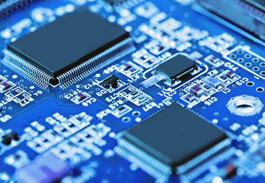
2. PCB Production—Multi-Layer PCB Production
Manufacturing a multi-layer PCB required similar stages that a single-layer PCB needed.
However, these stages need to be performed with a greater degree of accuracy and manufacturing process control.
Multi-layer PCBs are made using individual boards, one for each layer, that are much thinner.
These individual boards are bonded together to produce an overall printed circuit board.
Therefore, the individual panels must be lighter to prevent a thick finished multi-layer PCB.

3. PCB Production—Materials For Printed Circuit Boards
PCB can be made from a variety of circuit board materials.
► FR-4:
FR, or fire retardant material, is one of the most standard glass laminated materials made from glass-epoxy compounds.
Resin binder gives this composite material its flame-retardant qualities. The FR-4 material is used to design a highly dense or multi-layer PCB.
Its ambient temperature is between 120 degrees to 130 degrees C, according to the thickness of the substrate.
This material has the following properties:
- Good mechanical strength
- Low moisture absorption
- High electrical insulation
- Good fabrication capabilities
- PCB layers: 1 to multi-layer
► FR-5:
This glass fabric-reinforced material is perfect for high-temperature and humidity applications.
This is due to the presence of epoxy resin binder in this substrate. FR-5 exhibits:
- Excellent mechanical properties
- Good dielectric constant
- Low moisture absorption
- High chemical resistance
- PCB layers: 1 or double layer
• FR-3:
This fire retardant material uses stiff paper and epoxy resin binder for its composition.
• It is cheap and, therefore, an excellent choice to use for consumer electronics.
• PCB layers: 1 or double layer.
► FR-2 and FR-1:
FR-1 and FR-2 feature the composition of the stiff paper and a phenol compound.
Both are the same substrate materials, having similar characteristics. However, there is one difference which is the glass transition temperature.
FR1 has a higher glass transition temperature of 130 degrees C instead of 105 degrees C for the FR-2 substrate material.
► CEM materials:
Composite Epoxy materials, CEM, feature the composition of epoxy synthetic resins and materials produced from woven and non-woven glass fabric.
There are five types of CEM materials. CEM-1 is an FR, flame-retardant material featuring a composition of two layers of woven glass fabric, phenol compounds, and cellulose paper laminate.
CEM-2 is a good choice for a single-sided printed circuit board because it is composed of a single-layer woven glass fabric and a cellulose paper core.
CEM-3 and CEM-4 have similar characteristics.
It is commonly used in double-layer printed circuit boards and is a good choice for the FR-4 substrate. CEM-5 features material of polyester woven glass core and is not flame retardant.
Among all the mentioned circuit board materials, FR4 is the best circuit board material for PCB production. Other materials are suitable and low-priced.
However, they can only be used to make a single-layer printed circuit board, and their reliability is not good.
Therefore, FR-4 is best suited to make a quality superficial one layer to the multi-layer board.
4. PCB Production–Factors Affecting PCB Cost:
Always consider these factors for estimating the cost of PCB production.
1. Number of boards: Smaller printed boards are quickly processed in more significant numbers on the production panel, thus decreasing the cost per board.
2. PCB thickness and number of layers: The layers in the PCB also affect the price. More layers in a PCB means more thickness and complex WellPCB.
We will provide you with a one-stop service and high-quality products. You can send us the documents you need to make and get a quote immediately!
What are we waiting for? The PCB manufacturing process takes ten years, which is expensive. Therefore, design a PCB with a minimum number of layers and thickness.
The specification also affects the thickness of the PCB. For these boards, expensive materials increase the price. Furthermore, copper weight also increases the cost of the PCB.
3.PCB size: The price of a PCB usually exceeds its size.
The reason is that larger PCBs require more substrate material and holes of different sizes that increase the overall cost.
On the other hand, smaller PCBs are quickly processed in more significant numbers on the production panels, thus decreasing the cost per board.
4.Impedance control and routing: Routing and impedance control in the PCB adds an extra cost to the final PCB’s overall cost.
5. Solder mask and silkscreen: These additional items tend to increase the cost of PCB.
Therefore, the price decreases significantly if these features are not included in the PCB.
PCB Production–Conclusion
When you order PCBs from wellpcb.com, you pay a reasonable cost for high-quality production. We have WellPCB.
We will provide you with a one-stop service and high-quality products.
You can send us the documents you need to make and get a quote immediately!
What are we waiting for?
We have ten years of PCB manufacturing equipment and facilities that make us capable of producing 2 to 32 layers of PCB.
We made PCBs from Gerber 274-X data and drill files. It is used to make one layer in a physical board, and then multiple layers are bonded to form a multi-layer PCB.
Our expert team ensures that the PCB delivers what we promise.
Representatives are available 24/7 to help consumers decide on the best package that suits their budget without compromising the quality of the PCB.
Our team guides for appropriate options selection of competitive prices by giving reasonable suggestions for a considerable reduction in total costs.
We always try our best to deliver PCBs at an economical rate so customers can focus on their core purpose rather than worrying about the cost.
For more information, please contact our support team at [email protected].


