Of course! PCB Manufacturing Process, The Printed Circuit Board manufacturing entails quite many processes. That is why we would be taking another moment to enlighten you and guide you in making the right choice. Since we want to believe that this might no longer seem new in one way or another, we would love to get our customer’s feedback later.
Are you the type that prefers good quality PCB? Then this might be your long-awaited article. Also, at the end of this information, we would guide you through the necessary steps you need to make the difference to make you achieve the best.
Contents
PCB Manufacturing Process
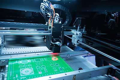
Several steps must be followed to achieve the desired or optimum result in manufacturing the printed circuit board. The manufacturing process insinuates the procedures needed to be followed in the production of the printed circuit board. There are several phases in the manufacturing of the printed circuit board. The early part of the manufacturing begins with using a computer to make the design through specific software. The second half of this article will describe this in more detail.
Computer-aided manufacturing (often called CAM) performs some operations, and these include:
- The input of the fabrication data
- The data verification
- Compensation for deviations in the manufacturing processes (ne.g., scaling to compensate for distortions during lamination)
- Panelization
- The output of digital tools (copper patterns, drill files, inspections, and so on.)
In the panelization process, some small PCB are brought together to merge them as a panel. We refer to an n-panel as one that comprises of a design duplicated n-times.
Another type is the multi-panel; the multi-panel brings together some different panels to form a single committee.
We also have copper patterning, and this is an initial procedure done by replicating the pattern in the fabricator’s computer aid manufacturing (CAM) system on a protective mask on the copper foil printed circuit board layer. Successive etching processes aid the eradication of unwanted copper. The chemical etching is carried out with the aid of a chemical known as ammonium persulfate. For projects related to PTH, additional procedures of electroless deposition are carried out, succeeding in the drilling of the hole.
After this, the thickness is increased or built by electroplating copper. Also, for small-scale projects, immersion etching is commonly used. The immersion etching uses a chemical such as ferric chloride, with the board being submerged in it. The disadvantages attached to this process are that it takes a much longer time when compared to the other method. Agitation and heat can be applied to the bath to fasten the rate of etching.
Flexible PCB Manufacturing Process
Unlike designing the device to conform to the circuit board, the flexible PCB allows the circuitry to fit electronic products.
2.1: PCB Manufacturing Process—Advantages of flexible PCB
Some of the advantages offered by the WellPCB offers DC motor controllers in both domestic and international markets. We have a flexible would be briefly discussed, and they include:
- Reliability: the flexible PCB is well known to be highly reliable since they do not comprise of many potential sources that may fail.
- Space: the flex design requires a minimal amount of space
- Cost-friendly: the materials required for the flex design is relatively reduced.
PCB Fabrication Process Steps
You might have come to understand the fact the PCB holds some advantages of the breadboard, and some benefits of these advantages include; high density offered by the PCB, unlike the breadboard, high reliability of the PCB compared to breadboard, the addition of odd components on the PCB which is technically impossible on the breadboard, and so on.
In a broad sense, As we all know, no PCB can be referred to as being standard; that is, they all have a different use for a product, and therefore the procedures involved in the production of the Printed Circuit Board vary and more complex. In a short while, we would be discussing the processes involved in the production of the PCB.
1: The first thing that comes to mind is deciding what kind of electronic circuit to design on the printed circuit board.
It is an essential aspect of PCB manufacturing. With the aid of your computer, make your preferred designs for your board with software like EAGLE – although there is other software you can use.
2: Print out your design on a suitable type of paper using a printer – laser printer.
Ensure that it is possible to fit in all the components on the print, with the size of the layout equivalent to that of the PCB. Make sure that black ink is used, and avoid taking the photo immediately after it comes up; wait for some while and allow it to dry. Although there are other methods compared to the one mentioned above, this is also good.
3: Trim out the layout without cutting the blank spaces along.
With the aid of an iron box, apply heat to the printed circuit board with the paper layout on top of the PCB. While you use the heat and pressure, ensure that the PCB maintains its position, and after a few minutes, you would notice that the board and paper are now attached to the layout. That is, when you cut, only cut out the form leaving behind the blank spaces. Since the article must be excluded, deep the board into the water for some minutes and peel out the paper. To remove more minor bits of the report, soak again for a few hours and remove the paper bits.
4: the next step is to etch the PCB.
It can be done with the use of a chemical known as Ferric chloride to remove excess copper. Immerse the board into the solution and let it maintain motion. When you can no longer see the copper layer, please continue to check and remove it. Apply little acetone on the PCB to get rid of the black color.
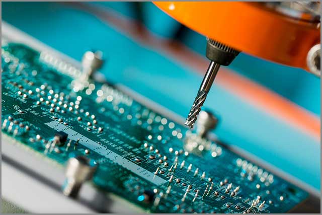
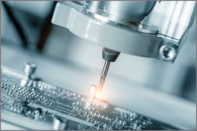
5: the next step is to drill the holes, and this can be done using a Dremel drill press depending on the size of the project.
In other instances, automated drilling machines are utilized for big-sized projects. The surface of the material is coated with gold, nickel, and so on.
6: the last step involves the use of solder resists covering the portions that are not soldered.
It is then tested and assembled.

PCB Fabrication Process Technology
The technology of the PCB has continued to progress with time. There has been a significant improvement in aspects relating to semiconductor improvements, miniaturizing, and so on. The PCB has successfully been able to meet a wide variety of needs or requirements. The manufacturing of PCB depends on some techniques that go along with plating, etching, use of the machine, and so on. When we mention these different techniques, you would understand that each of them has its unique cons and pros, and one important thing to note in the manufacturing of PCB is the accuracy of the equipment.
4.1: an Imaging technique
One of the initial methods used in imaging is screen printing, with advantages that include;
- Suitability for a large project
- Not very costly
- Low material requirements
- Specialized screens, and so on.
An accurate method for depositing circuit images on board is through photoimaging. The photo imaging is identified with cons which include; tool wear, stress relaxation, and so on.
4.2: PCB Manufacturing Process—Plating technique
Generally, this technique deals with the application of metal finishes to a PCB. Under this technique, we have; Electrolytic, Electroless, and Plasma plating.
4.3: Laminating technique
A laminating technique is the hydraulic hot press method, which was a common type but has been improved by continuous developments. This technique is used in producing the circuit board, alongside the production of multilayer circuitry design.
4.4: PCB Manufacturing Process—Etching technique
The etching technique majorly bases on the extraction of excess metal from the PCB surface to attain a leveled surface. The different chemicals used for etching include cupric chloride, peroxide, and nitric acid.
Best Manufacturing Process PCB Fabrication Specification
As the importance of the heart to the body, the Printed circuit board is that important to every product that has to do with electronics. The printed circuit boards are concerned with parts or components that give internal instructions to your products, and they are designed in many shapes and sizes.
The fabrication specification can be said to be the design requirement that is not concerned with the behaviors or function but rather determines the manufacturability, cost, etc.
5.1: What to note about the fabrication specification
Size: the size refers to the dimensions of the printed circuit board. At this stage, it is necessary to note that the cost of the printed circuit board varies with the size of the surface area. If we compare an irregularly shaped printed circuit board to a small rectangular type of the same board, the irregularly shaped PCB will be more costly than the latter. So to level the price, it is essential to use the space wisely.
Complexity: the number of layers measures the complexity of the PCB.
Type of material: in one way or the other, we must have heard about the glass epoxy which is otherwise known as the FR-4.
A few years ago, the FR-2 was used (FR means flame-retardant, with the number insinuating the flammability) and otherwise referred to as the phenolic paper. Unfortunately, this material wasn’t a good choice due to the cons: toxicity and cracking. These days, the most common type of material used is the FR-4, and many PCB designers prefer the FR-4 as the first option. Apart from the standard variety of printed circuit board materials, other materials are relatively less common, including PEEk, polyimide, and Teflon. Still, considering the thickness of the material, it must give the most excellent attention.
The thickness of the board: in a way, the thickness of the panel is decided by the number of layers, about the PCB designers deciding on the dimensions that result in the consistency. The thickness of the board is an elementary mechanical specification of the printed circuit board, and sometimes, 1.6mm seems to be the standard. The designer is responsible for selecting the dimensions that will suit the preferred thickness. For thickness ranging from 1.0mm and below, a small spaced PCB is likely to be in question.
Plating: Know the flex PCB materials. Place the layers of flex in the center of the stack-up to protect outer-layer leaf refers to the situation in which copper surfaces that are not covered with another metal material increase the level of solderability when assembly operation is completed. Hot Air Solder Leveling is a common type of plating, and we also have other types of the plate, including ENIG (Electroless nickel immersion gold is a more costly leaf but, of course, gives a better result).
5.2: Checking For Design Rule Violations
Immediately you know your way around fabrication specifications, it is necessary to go along with the specification all through the development process.
Multilayer PCB Fabrication Process
The external coatings of our multilayer comprise sheets of glass cloth that are pre-impregnated with uncured epoxy resin and a thin copper foil. Generally, the multilayer printed circuit board depicts that the PCB, when counted, contains more than three layers. Between each layer are insulating materials that have been prepared with the multilayer printed circuit board making use of some double-sided PCB.
In situations where the dependability of the metalized holes concerned with the printed circuit board manufacturing are to be made better, materials with heat-resisting ability and firmness on dimension should be used by the multilayer PCB designers. When counting the layers of the multilayer printed circuit board, it is often found to be even.
There are some processes related to the fabrication of the multilayer PCB. The printed circuit board designer or manufacturer should first create an inner core layer image on the middle ground. After that, merge the inner core with maximum temperature and pressure with the aid of a pressing machine. The manufacturing processes are alike for the production of outer layers compared with the double-sided printed circuit board.
6.1: PCB Manufacturing Process—Lay-up and Bond
The mechanic (otherwise known as the upper operator) will place some material on the large steel floor: the copper foil and two prepreg sheets. After successfully doing this, he positions the previously treated core on the alignment pins and joins another prepreg sheet (2) with copper foil and an aluminum press plate. Having done this, he constructs three panels on the base plate using the same format and rolls the massive stack under a press. The steel top plate lowers, stack together, and the complete stack is rolled out. Three stacks are collected on a loader by the machinist and loaded into the bonding press. The press has been designed to bond the layers of the printed circuit board together by utilizing the heated press plate and pressure.
Conclusion
If we are responsible for your PCB, then this only means that you prefer a high-quality type, as this is what we offer. We have taken you through the internal and external information concerned with the WellPCB. We will provide you with a one-stop service and high-quality products. You can send us the documents you need to make and get a quote immediately! What are we waiting for? We have ten years of PCB manufacturing processes, and the least we can now do is give you the very best of your desired product.
We have mentioned different subtopics under this article, and we now believe that it would enable you to make the right choice and bring you back to us.
Why don’t you contact us today and secure your interest in high-quality products? Also, you can request a quotation, and in case you have troubling questions or suggestions, please feel free to pass them across.


