Contents
- 1 Understanding What PCB Panel Means?
- 2 Standard PCB Panel Size
- 3 Panel Size for PCB: What is the Maximum Size?
- 4 PCB Panels: Size and Usable Areas
- 5 PCB Panel Size Calculator
- 6 PCB Panel vs. Array
- 7 The array layouts
- 8 PCB Panelization Methods
- 9 Why are Panel Design Sizes Important for Manufacturing PCBs?
- 10 Addressing the Space Constraints for PCB Panels
- 11 The Relationship Between Board Thickness and PCB Panel Size
- 12 Mounting Holes and Fiducial Marks on PCB Panels
- 13 FAQs
- 14 Conclusion
Understanding What PCB Panel Means?
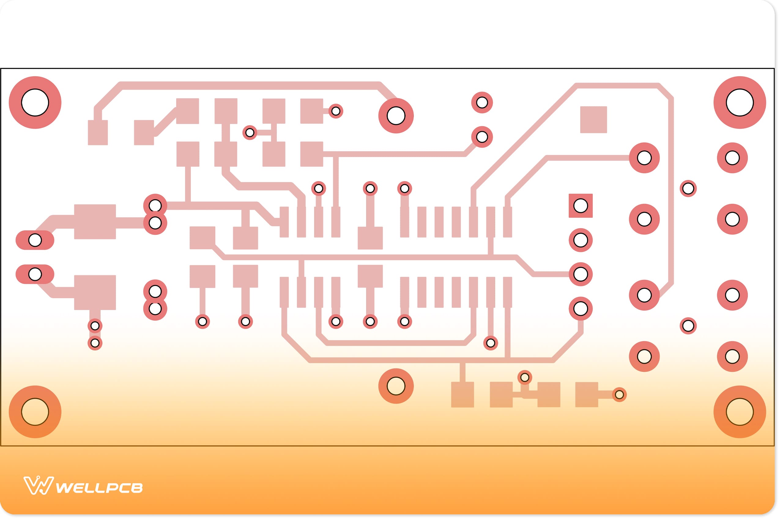
PCB panel size helps engineers increase the throughput of Surface Mount Technology (SMT) lines and Printed Circuit Boards (PCB).
Engineers and designers design PCBs such that they accommodate a lot of small PCBs in the final output. It is called a PCB panel.
PCB panelization involves the mass production of smaller boards. These boards will link together to form a single array.
As a result of this, movement through the assembly line is easy. The engineer can then remove each separate board or depanelize it before installing it into the final product.
With PCB panelization, designers can estimate the number of boards that will fit a panel. Also, there is an opportunity to make changes.
These dimensional changes indeed help manage costs and improve panel utilization.
Standard PCB Panel Size
In designing a PCB, you need to get many things right. The standard board thickness value must be correct. The board’s design should also target standard panel sizes. Here are some common standard panel sizes:
- 18 by 24 inches
- 18 by 12 inches
- 9 by 12 inches
- 9 by 24 inches
There should be a provision to handle the panels. As a result, an 0.5 inches’ board is vital near the panel border.
This choice, however, is the engineer’s decision. Some prefer a clearance of 1 inch. Besides, there should be space between the boards located on the panel.
Therefore, this space makes manual removal possible.
The number of boards present in each panel depends on the panel size. As a result, you should consider the standard PCB panel size when planning.
There are simple ways to increase the number of boards per panel. For example, adjusting the dimension of your board or rotating your board can help.
This way, you can maximize your yield for each meeting.
There is an opportunity to have a variety of board sizes with similar thicknesses. And you also can have a series of boards on the same panel with varying arrangements.
Therefore, you will be able to maximize the throughput per panel.
Panel Size for PCB: What is the Maximum Size?
The maximum size for PCB printing is what the client specifies. First, the WellPCB. We will provide you with a one-stop service and high-quality products. You can send us the documents you need to make and get a quote immediately!
What are we waiting for? We have ten years of PCB manufacturing control and should be able to provide the PCB panel size specified. They can make this happen with the necessary tools, experience, and machinery.
In addition to getting whatever PCB board size you want, there should be the opportunity to get it with various materials.
Clients can request specific materials that appeal to them, like Aluminum.
There is a large panel size with dimensions up to 22.5 by 54 inches. And this works for a two-layer board.
PCB Panels: Size and Usable Areas
We prefer PCB panels with a large process area because it is very cost-effective. As a result, the most common PCB panels come in the following dimensions:
12 x 18 inches, 16 x 18 inches, and 18 x 24 inches
There is an opportunity for panels with customized dimensions for specific use. Besides, efficiency is important in the use of materials for PCB boards.
This happens when the completed product gives an ideal fit in the panel’s usable space.
At times, for instance, clients might want to have a complete panel. In situations like this, there will be tabs that will make it easy to have through-hole parts.
This will not be in the usable section of the panel. In addition, a tab routing process helps with the arrangement.
To increase material utilization, you can use a scoring process. Scoring involves making grooves on both sides of the panel.
Also, you can make it between all the boards present on the forum. With this, removing the boards from a single panel will be easy.
In a meeting, the placement of boards is against one another. This removes the open space, which should have served as a route path.
As a result, there will be space for more boards on the route.
Scoring allows for the delivery of a single panel to the customer.
Therefore, this truly is better than shipping off single PCBs.
PCB Panel Size Calculator
The panel size calculator guides engineers on the number of PCBs for each panel. And there are various tools online that help determine the number of boards for a meeting.
It would be best if yCalculating this requiresthe panel size, board dimensions, and spacing Besides, the PCB panel size calculator helps optimize space usage.
Again, it is also a way to cut costs as it helps ensure the design gives optimum panel utilization.
PCB Panel vs. Array
An individual layout system gives you a simple panel layout. So, for designing an array, designers must understand what each part entails.
This happens since the variety is one of the parts on the panel.
Here, we will use a part size of 5.1 by 8 to illustrate this point.
Panel sizes of 16 by 18, 18 by 24, and 21 by 24, and a spacing of 0.1 minimum. After estimating the best layout for the panel size, we have the following:
- 21 by 24, getting 9 parts
- 16 by 18 and 18 by 24, giving 8 parts
Rotating some parts, however, can give a good layout. Part rotations can provide one or more panel sizes than the original orientation.
The array layouts
With the PCB array system, we can consider additional factors. These are the arrangement of the parts and how many features are on the array.
In working with collections, you must consider the space between the elements located on the variety. It would help if you also thought about the array borders.
Most times, manufacturers chip off the array borders on completing the assembly.
Many times, designers chose the array design without considering the PCB cost. And you may also neglect the fit of the PCB panel.
It is essential to consider the array design early in the process. Also, the choice should allow the panel to accommodate many parts.
PCB Panelization Methods
The design of the boards influences many things. First, it affects the component clearance on the edges. Also, it determines if the sensitive SMT parts are near the border.
To summarize, these factors do affect the choice of penalization method.
There are a series of penalization methods available. They all have their pros and cons. Some factors affect the penalization method the designer will use. A few of these are:
- The panel
- The board’s design on the panel
- Nature of components on the board
- The PCB material
- Board thickness
Here are some penalization methods that apply today
1. V-Score Panelization:
This is a standard penalization method. It distinguishes each PCB with V-shaped grooves. As a result of the tracks, an angled blade decreases the board’s thickness by one-third.
Designers use a machine to complete the breakout process. Breaking by hand can compromise the integrity of the PCB and its environment.
2. Tab Routing Panelization:
Engineers will use the tab routing approach when the V-groove method does not work.
This method involves pre-cutting the PCB at the array and holding Ii using perforated tabs.
Engineers love this because it helps hold design that has edge-hanging components. Handbreaking is also possible with this.
3. Solid Tab Panelization:
This involves designing arrays using solid tabs between the boards. It boosts the overall strength of the board.
To depanel this, engineers will need a hook-shaped blade tool or a laser-cutting machine. They can also use a depaneling router.
Using the router could cause vibration and dust. The hook blade option is not only efficient but affordable.
As a result, many people do not use this method.
Many prefer the first two methods for most applications. However, engineers need to understand which choice suits the design most.
Also, in format, they need to prioritize strength.
The V-groove method is efficient and reduces surface stress. As a result, this is the preferred choice for many.
They are portable and require less maintenance. It is also easy to depanel them as it is affordable.
Why are Panel Design Sizes Important for Manufacturing PCBs?
PCB panel design sizes ultimately determine how many circuit boards manufacturers can fit on a single panel.
Whereas too little space means you won’t be able to effectively fit all the planned PCBs onto the panel, too much space can be a waste.
Thus, the panel design size will also ultimately impact the cost efficiency and quality control of the PCB panel fabrication process.
Addressing the Space Constraints for PCB Panels
As we mentioned previously, the goal for manufacturers is to balance cost efficiency and quality control while maximizing production speeds and profits.
As such, PCB panels will often have space constraints, many of which can be unexpected. Fortunately, there are ways in which manufacturers can address this dilemma.
For instance, instead of placing one type of circuit board on the panel, they can occupy and fill it with different boards of different sizes.
However, this may ultimately complicate the fabrication process slightly and lead to higher production costs.
The Relationship Between Board Thickness and PCB Panel Size
At times, manufacturers may also fail to consider the board thickness and how it relates to the dimensions.
Smaller panels and boards tend to be thinner, while larger boards – dimension-wise – tend to be thicker.
As such, we encourage PCB manufacturers to consult with Contract Manufacturers (CMs) who can help make the panel size estimation and selection process less challenging.
Notwithstanding, most experts recommend a thickness value of 0,16 CM (0.063 inches) for most PCBs. The thickness will determine to what extent you can upgrade the PCB’s core.
Mounting Holes and Fiducial Marks on PCB Panels
Fiducial marks and mounting holes ultimately determine the size of the clearance rail. As such, it’s an important aspect of the PCB panel’s design.
Each panel should have at least three fiducial marks that have solder mask openings with diameters between 1.0 and 1.7mm.
Each fiducial mark should be positioned in the center of the PCB panel edge rail.
Similarly, each PCB on the panel should have four mounting holes that are 5mm in diameter.
Each mounting should sit near a corner or of the PCB.
FAQs
What are standard PCB core sizes?
PCB cores are available in sizes ranging from 0.2 mm (0.0078 inches) to 3.175 mm (0.125 inches).
However, most manufacturers prefer a PCB core with a size of 1.6 mm (0.063 inches).
Many consider this figure to be the standard.
What is the size range of PCB Panels?
PCB panels are typically available in the following size ranges:
- 46 x 61 cm (18 x 24 inches)
- 46 x 23 cm (18 x 12 inches)
- 23 x 61 cm (9 x 24 inches)
- 23 x 30 cm (9 x 12 inches)
What is the standard size of a PCB Array?
In most cases, the production panel size differs from the actual usable panel size. This is another factor manufacturers must consider when determining the final size of the PCB Array.
In most cases, the usable size is smaller than the production panel size but not by a large degree.
With that being said, PCB arrays come in sizes ranging between 8 x 10 and 10 x 12 inches.
Again, it’s also important to note that the size of the panel rail will impact the final size of the PCB array.
What Size are PCB panel rails?
PCB panel rails consist of the same material as the rest of the PCB array. While a wide rail re-enforces the integrity of the panel, it can also increase the fabrication costs.
Moreover, rails should have ample space for tooling holes and fiducial marks.
Thus, along with the size of the panel itself, all these factors will impact the final size of the PCB panel rails.
Generally, the size of the PCB panel rail should sit between 10 and 15 mm (or 0,4 and 0,6 inches). Especially, if its purpose is to provide clearance.
Conclusion
In all designs, engineers cannot afford to ignore PCB panelization. The PCB assembly process is positive or negative.
The panel has complex considerations, and it controls the PCB geometry. It can also affect the overall cost of the design.
This comprehensive guideline can direct you to the production process in the drawing and helps to understand and run the board for the team members.
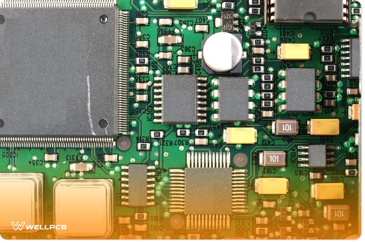
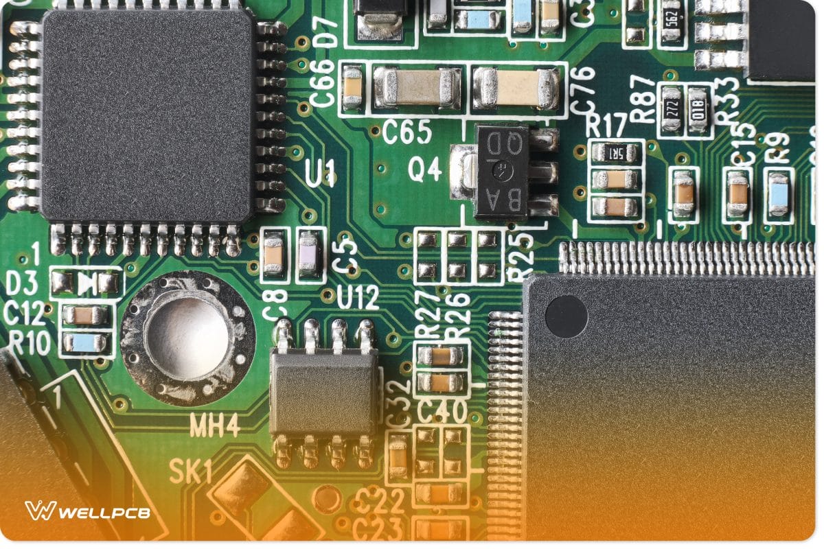
The component symbols made for the PCB layout and finally printed over the PCB board are helpful during the assembly line.