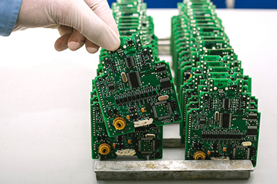
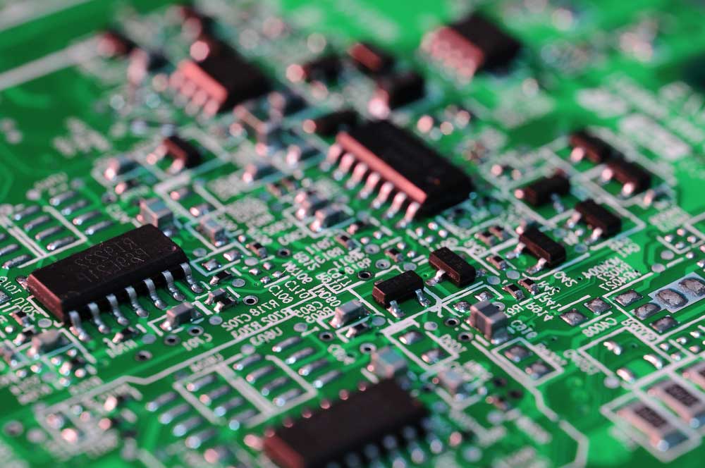
Printed circuit boards are considered to be a linchpin in the current electronics available in the market. In situations where a gadget is required for computation, even with necessary things such as a digital clock — odds are there that there’s a PCB within it. PCBs, breathe life into gadgets by steering electrical signs to fulfill the gadget’s electronic necessities.
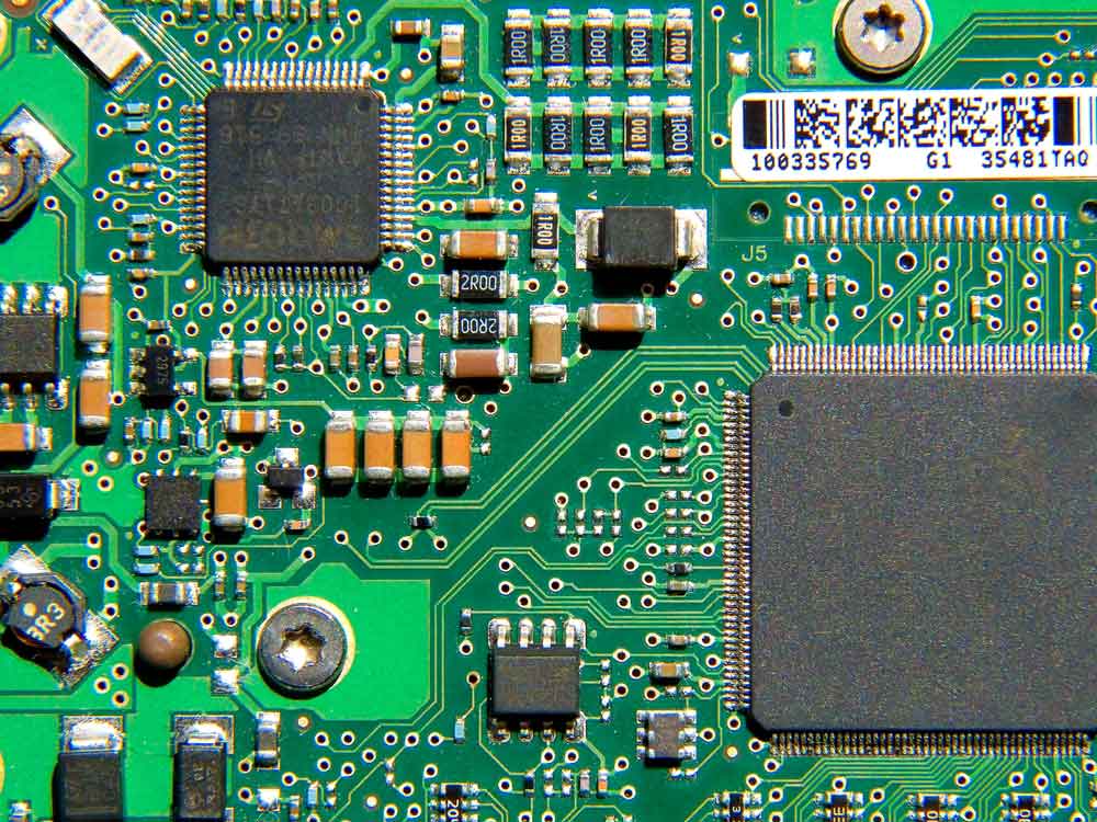
To achieve this, Circuit boards are made to consist of a system of ways that need to adhere. The copper pathways enable circuit boards to supply direct electric current to all sections of the PCBs. Three kinds of PCBs are manufactured. It is hence, essential to comprehend the comparison between each of them to be able you choose the correct PCB that meets your needs. To better understand a PCB function, we’ll stroll onto how to manufacture a PCB, thus making it for you as a PCB shopper.
How to Manufacture a PCB for the PCB shopper
The main steps followed in the manufacture of PCB are the following:
►PCB Shopper— Developing the design of PCB
To initiate the process of PCB manufacture, you must develop the plan first. The most utilized design software utilized by PCB architects is called Extended Gerber, otherwise called IX274X. Regarding PCB configuration, Extended Gerber is an excellent bit of programming since it likewise plays output design. This Extended Gerber transforms all data in a coded form that the originator needs.
►PCB Shopper— Pre-bonding the Copper used in inner layers
The third step becomes the initial phase of the manufacture of circuit boards. As soon as the design of PCB is laminated, the manufacturer has to pre-bond it to the lamination, which fills in as the circuit board structure. The manufacturer then removes copper to uncover the diagram from prior. Next, the overlay board is secured by a kind of delicate photograph film referred to as resist. This element enables experts to get an ideal combination of the photographs of the diagram and the printed material to the photoresist.
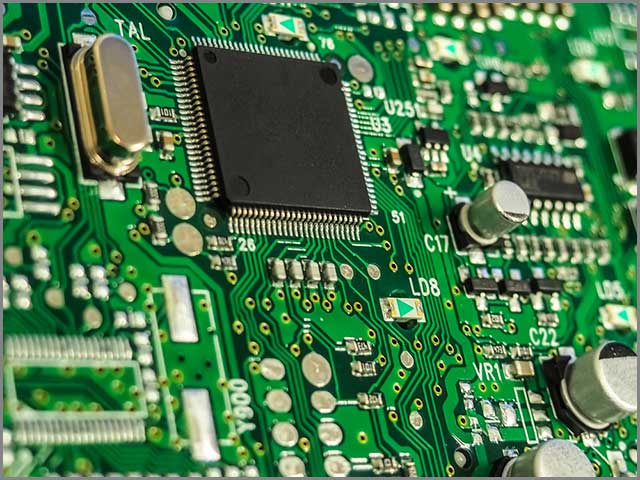
►PCB Shopper—Inspection and Layer Alignment
The optical inspection and proper is amazingly imperative because once the layers are aligned and laminated, any mistakes that exist can’t be amended.
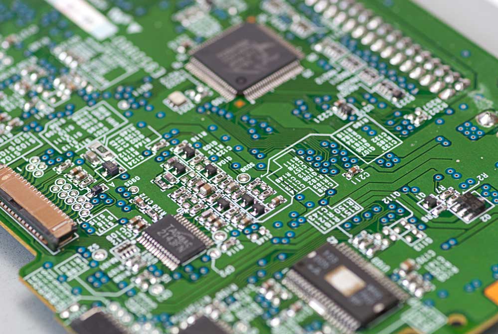
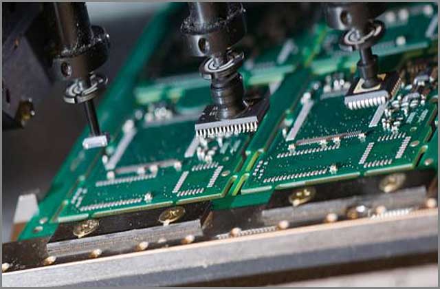
►PCB Shopper— Drilling
When preparing to drill a PCB, X-ray machines are utilized to find the spots for drilling. At that point, you should make guiding holes to secure the circuit board stack before drilling more holes. With regards to penetrating these drills, a computer-based grill is utilized in drilling holes, using an Extended Gerber plan to provide guidance. On completion, any extra copper that is left on the surface is scraped off.
►PCB Shopper— PCB Plating
Know the flex PCB materials.
Place the flex layers in the center of the stack-up to protect outer-layer plating procedure utilizes a synthetic to meld the PCB layers together. Upon being cleaned, the circuit board is then bathed with chemicals.
►The Last Etching of the Layer
Regarding the etching of the PCB outer layer, a tin guard is utilized to help ensure the copper amid the etching procedure. When all the unwanted copper is evacuated, the PCB’s associations have been appropriately established, and it’s prepared for solder masking.

Conclusion
The other steps include applying the solder mask, finishing the PCB and silk-screening, electrical reliability testing, and lastly, cutting and profiling. These further steps are essential from the manufacturer’s point of view and not necessarily described in detail for a PCB shopper. The process mentioned above appropriately understood is sure to persuade you as a shopper to decide and purchase a PCB if deemed necessary.
For PCB shoppers, the best destination is the WellPCB. Just visit www.wellpcb.com and submit the PCB Gerber file to get the customized product within a brief period.
You can learn more from this video: