Contents
What is PCB Stencil?
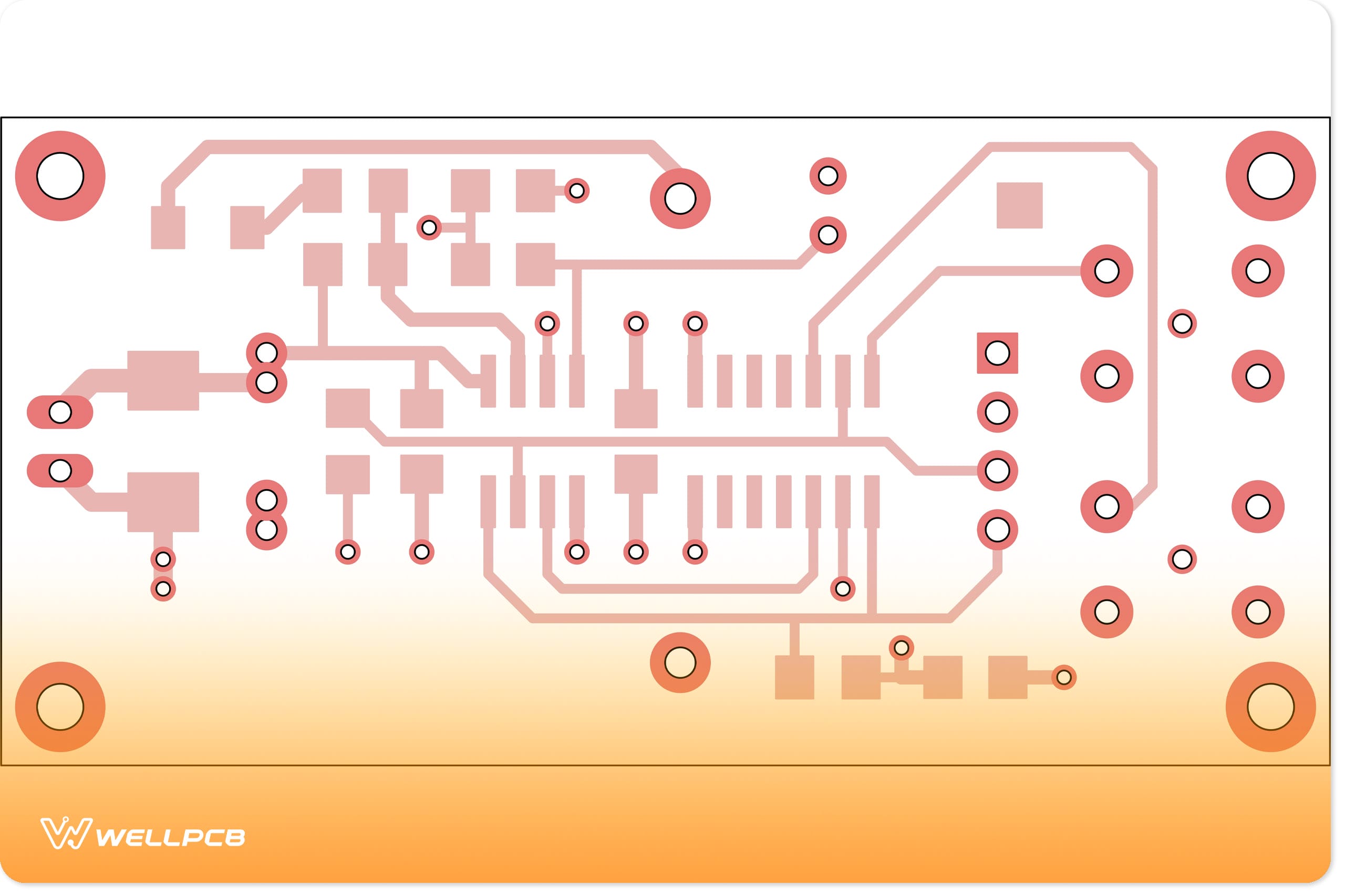
A stencil is a thin sheet of material bearing a formation of apertures that determine the layout of components on the PCB. With the solder stencil, you can deposit the appropriate quantities of solder paste with flawless precision in one go across the board.
Your board becomes set for the installation of the SMD once you apply solder paste over a PCB pad covered with the stencil. When you remove the stencil, the solder paste deposit sits on the board according to the formation of the stencil’s apertures.
The flawless deposition of solder paste ensures the solder joints are optimal regarding mechanical strength and electrical connections.
Now, most suppliers of PCB pads also produce PCB stencils. When you order from such suppliers, they give you the option to collect your PCB together with its custom stencil.
Nonetheless, there are two types of stencils: the framed and the frameless. While the frame-less are cheaper and easier to store, they’re the second-best for use in high-volume printing.
The stencil’s material is a primary determinant of its capacity to release solder paste through the apertures. You’ll find out more about this in the subsequent sections of this guide.
However, you can improve a stencil’s paste-release capacity by applying a specific type of coating on it.
PCB Stencil Design
The following is a breakdown of the critical elements of stencil design:
Stencil Thickness
It is another crucial determinant of a stencil’s capacity to release the solder paste. If the thickness isn’t suitable for the size of apertures, you’ll not achieve the required solder joint. In this case, the paste may adhere to the inner walls of the cracks due to surface tension. The following is a breakdown of critical factors that you should consider when selecting your stencil thickness:
Aspect Ratio
The thickness determines the quantity and height of the solder paste that forms a solder joint. The lower the amount, the higher the possibility of disconnects and the lower the possibility of jumpers.
This correlation, called ‘aspect,’ results from the differences in forces acting on the paste as it glides through the aperture. These include the force that pushes the paste beyond the opening and holds the paste within the gaps.
The contrast between these two forces is represented by a measurement known as the Aspect Ratio. To achieve optimal paste deposition, you need to ensure that the Aspect Ratio is more significant than one.
The surface tension between the paste and the pad must exceed the one between the paste and the aperture wall. The Aspect Ratio can be deduced by determining the ratio of the aperture width to the stencil’s thickness (W/T).
Nonetheless, industry standards define the criteria for determining the stencil thickness best suited for an aperture size. The lowest bound of the industry standard for Aspect Ratio is 1.5.
Area Ratio
Another critical measure for determining how the thickness of a stencil affects its paste-release capacity is its area ratio. The area ratio is the ratio of the surface area of the aperture to the surface area of the aperture wall.
The lowest bound of the industry standard’s range of surface areas is 0.66.
QFP and BGA Pitch
Also, when determining the appropriate thickness for your stencil, you need to keenly consider the fine-pitch QFP, BGA, and smallest chip size.
For a QFP with a pitch ≤ 0.5mm, your stencil’s thickness should fall between 0.12mm and 0.13mm. A QFP with a thickness > 0.5mm requires 0.15mm – 0.20mm stencil thickness.
For a BGA with a ball pitch of 1.0mm +, the appropriate stencil thickness is 0.15mm. For a BGA with a pitch between 0.5mm and 1.0mm, you should choose 0.13mm for the stencil thickness.
It’s even more imperative to consider the BGA or the minor components if you’ll be placing different ICs simultaneously on the board.
SMT Stencil Sizes
The rules for the determination of the appropriate stencil thickness for an SMT assembly are more intricate. However, it’s also imperative to consider the aspect and area ratios when determining SMT stencil sizes.
For an SMT assembly that deploys chemical etching, the appropriate aspect ratio is 1:1.5. For laser-cut stencil pitch type; the proper aspect ratio is 1:1.12.
Moreover, now that you’re equipped with adequate information about the essential qualities, you’re set to explore PCB stencil makers. The next chapter shows you how.
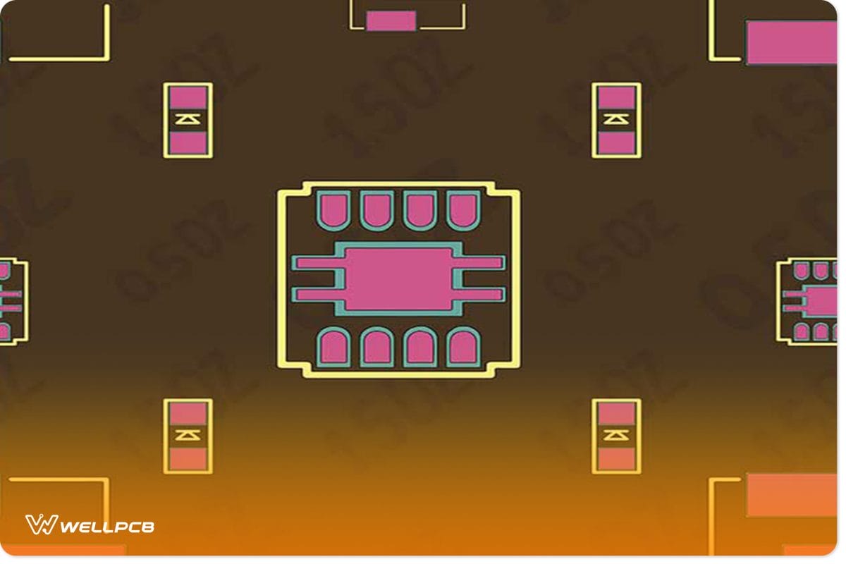
Aperture Design
The aperture design can affect the solder joints in many ways. First, it determines the chances of the occurrence of defects such as bridging and solder beads. It can also provide a gasket seal between the stencil and the PCB.
Alignment
It is the ultimate determinant of the precision with which you print solder joints on the pads. You can achieve excellent alignment by inscribing registration marks called fiducial marks on both the PCB and stencil.
The Stencil Material
The material is also as critical to the success of PBC stenciling as the PCB stencil design. The thin sheets are usually made of either metal or polyimide. Metal (typically stainless steel) stencils are the most ideal for producing numerous prototypes.
Stainless steel stencils allow for the formation of more accurate apertures. The molecular structure of stainless steel makes for much smoother aperture walls and will enable you to achieve an effective aspect ratio quickly.
However, since they’re more expensive, they’re more overkill for producing a handful of prototypes. Polyamide stencils are a much cheaper alternative. When delivered through a laser cutting technique, they can also make for excellent apertures.
Solder Stencil Type
There are two types of solder paste stencils: the framed and the frameless. Framed stencils, also called glue-in stencils, are stencil foils cut with a laser and permanently fixed in a stencil frame.
Framed stencils are the best choice when it comes to high-volume PCB printing. Since they usually come with very smooth aperture walls, they’re best suited for use when very tight pitches are required.
Frameless solder paste stencils, which are also produced through laser cutting, come with tensioning systems. With these tensioning systems, they don’t need to come fixed in a frame. It makes it much easier for you to store them.
They’re ideal for short runs of PCB production. They also have smooth apertures. Moreover, you can use them for PCB pads that require 16 Mil or fewer pitches and Micro BGA’s.

Solder Paste
The flux and the alloys in a solder paste can also impact the extent to which the solder joints hold components. If the change in the solder joint is insufficient, the solder won’t hold parts firmly on the board.
The Stencil Coating
There are various types of coating for PCB stencils that help tackle specific problems in PCB stenciling. For starters, it is pretty challenging to clean boards after large production runs.
You can easily wipe excess solder from the underside of a PCB to prevent the excess solder from smearing other boards. However, it’s excruciating to do the same in large production runs.
With certain types of coating, you can reduce the residual solder in the aperture walls that distort the required solder paste/flux formulation.
Now that you have a clearer understanding of the types and qualities of PCB stencils, you’re better off implementing PCB stenciling. The following chapter gives you a closer look at some essential equipment for making a PCB stencil.

Specific PCB Stencil Design
PCBs with copper pads that promote conductivity and heat dissipation in the PCB pads call for stencils with unique designs. In such cases, a stencil design for PCB boards without copper pads would lead to copper lifting and poor soldering of outer leads.
To eliminate such defects in such cases, you need to add a ‘window effect’ to the aperture design. That eliminates the defects by moderating the solder volume.
If the copper pads on the PCB pad come with vias that further enhance the dissipation, a different stencil design is required. The stencil’s design must prevent the deposit of solder paste in the vias.
There are also cases where a PCB pad requires the use of stencils of varying thicknesses. In such cases, there may be delicate pitch parts that need thin stencils and more significant parts that require thicker stencils.
You can meet such requirements by using multilevel stencils that have step-up and step-down areas. You can create step-up spaces by adding more material to a selected area of the stencil.
That increases the quantity and height of solder paste in the solder joints formed in that area. The opposite of this holds in the step-down room.
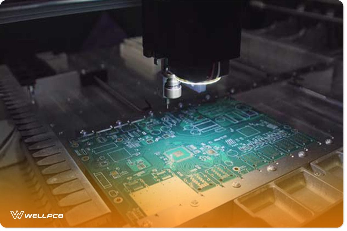
PCB Stencil Maker
It’s one thing to acquire a thin sheet of material with the right thickness. However, it’s a different ball game to punch holes of the perfect sizes in them. Given that a PCB stencil must bear hundreds or even thousands of holes aligned with high precision, it’s ill-advised to punch holes manually.
The three most widely used methods for making stencils with appropriate holes are chemical etching, laser cutting, and electroforming. Each of these methods can lead the surface of the pore wall to a different finish; the smoother the finish, the more efficient the paste release.
The most popular among these three PCB stencil makers is the laser cutter. In this chapter, we’ll show you how to make PCB stencils using a laser cutter. Note that this technique isn’t suitable for creating stencils that have very tight pitches.
PCB stencil laser cutter
It is a laser system that uses high-powered beams to punch holes in stencils according to parameters dictated by computer software.
It completely automates creating apertures in stencils, taking stress and margins of errors out of the equation. When you cut your PCB stencil using laser cutters, you can rest assured the edges and the aperture walls will be optimally smooth.
Stencil laser systems are usually highly versatile. With lasers, you can cut, drill, and ablate both stencils and PCB pads made of a wide variety of materials.
PCB laser cutters also carve stencils without producing dust, as with traditional mechanical cutting systems. It makes a whole lot of difference in PCB electronics that come with optical components.
Tools for this technique:
1. Laser cutter
2. Mylar sheets
3. ExpressPCB or EagleCAD software
4. ViewMate Gerber Viewing Software
5. PDF printing software
6. SketchUp, AutoCAD, or any software that views and edits .dxf files
The Steps
Stack the Mylar Sheet
Stack two Mylar sheets together. In this technique, you’ll be heating the Mylar sheets until the first sheet gets detached from the stack. In the process, the second sheet will absorb the melted pad of the first sheet, allowing the first to be pulled off cleanly.
Export the design file from ExpressCAD or EagleCAD:
In EagleCAD, export your top and bottom cream layers through a cam file, like you ship Gerbers for manufacturing. In ExpressPCB, open the File menu and select the “Export DXF Mechanical Drawing” option.
Swell pads in ViewMate
If you’re using software that exports Gerbers, you need to compensate for the melting induced by the cutting process. Since the melting will cause the pad size to enlarge, you need to preemptively cut down the pad’s size.
First, select File>Import>Gerber to import your cream layers into ViewMate. Next, choose Setup>D Codes. Select all columns in this area, and then open Operations>Swell. Type in the value for the size adjustments according to your laser specifications.
Afterward, print the Gerber to PDF and then save it.
Swell pads with Auto Cad
If you’re using ExpressPCB, you might also need to scale down the contents of DXF using different software. You can do that with AutoCAD. To do this, highlight all the drawings in the open AutoCAD window and then key in “SCALE.”
In the Scale Factor dialog that pops up, key in the appropriate scale figure. It will render the drawing in the proper scales.
Once this is done, print out the finished drawing to a PDF.
Cut the Stencils
Adjust the settings on your laser cutter accordingly to cut through the stacked Mylar sheets. The first sheet will melt a little due to the laser’s heat. However, the second will absorb the melted pad of the first, allowing you to pull out the first sheet neatly and efficiently.
So far, we’ve examined a widely used PCB maker. However, the type and qualities of your PCB stencil remain the most crucial determinants of success in PCB stenciling. In the next chapter, we dissect further the rates and types of solder paste stencils.
PCB Stencil Printer
PCB stencil printers are famed for their defect-free and repeatable printing capacities. These printers are usually ideal for both low-volume and high-volume PCB production.
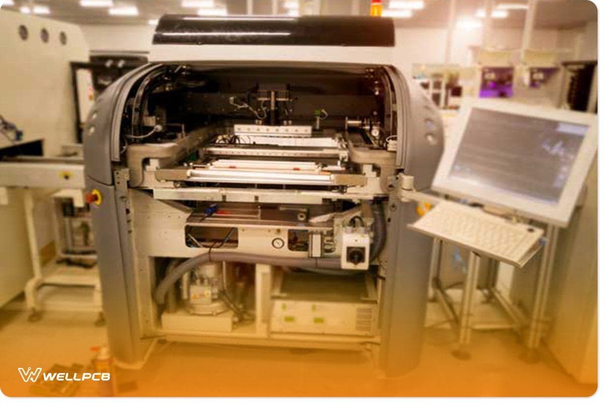
There are two main types of SMT stencil printers: automatic and semi-automatic SMT printers. There are also manual stencil printers designed explicitly for short-run and prototype production.
Some of the critical features of SMT stencil printers include a screwdriver, speed controllers, and camera systems that facilitate PCB alignment. The operations usually revolve around adjusting stencil size settings and the stencil placement on a frame mounter.
A typical printer allows you to set the print speed, stroke length, squeegee pressure, and more. SMT stencil printers also come with screens that display details of the operation.
They also come with compartments that wipe the underside of stencils through actions like wetting, drying, and vacuuming. The vacuuming steps expunge residual solder stuck in apertures.
Conclusion
There you go. We’ve just dissected PCB stenciling inside out and show you everything you need to know. Armed with this knowledge, you’ll be better off avoiding specific printing errors that might ruin your PCB project.
Moreover, you can reach out to us whenever you feel lost in the PCB manufacturing process. We have both top-draw expertise and state-of-the-art equipment to help you overcome any problem with the PCB stencil.