Contents
What is a Presensitized PCB?
A PCB, also known as a printed PCB, serves two primary purposes regarding the functioning of automated tools; it is a place used to mount the components and provides electrical connectivity between the components.
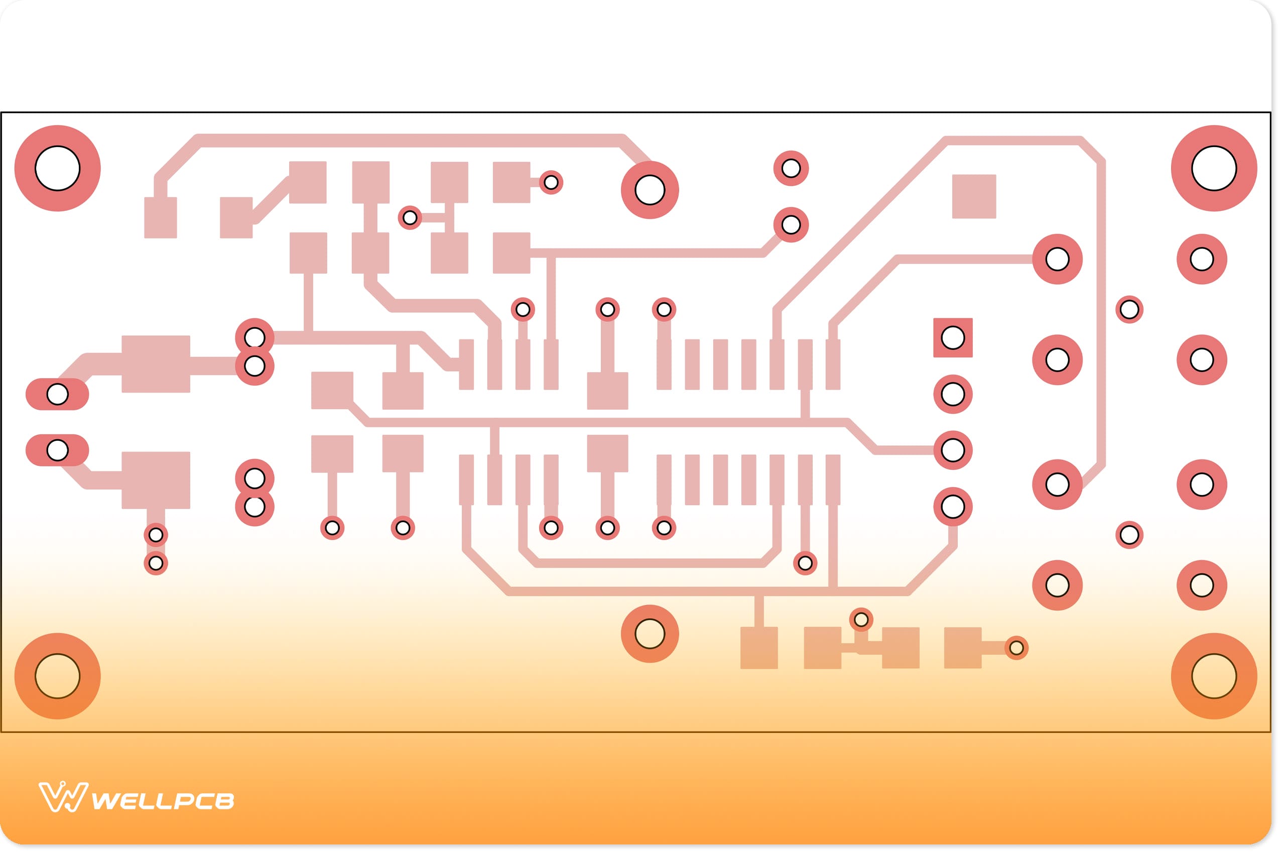
There are different types of PCBs currently in the market. Conventional PCBs and presensitized PCBs. A presensitized PCB is a factory-manufactured or professionally-made PCB whose surface has a coat with a photosensitive emulsion.
Today, almost every electronic product that is available in the market uses presensitized PCBs. Presensitized PCBs are one of the most common electronic devices used in plenty of electronic components currently available for sale in the market.
Design and Manufacturing Process of Presensitized PCBs
Are you thinking of creating or building your PCB in the same manner professional companies do? Perhaps you have an electronics project in mind. If so, then relax as you have come to the right site. The following is a step-by-step guide to coming up with your PCB board. Let’s begin!
Items to Buy
Are you feeling ready enough to create your presensitized PCB? If so, there are several things that you need to purchase. Here is a breakdown of what you need to buy:
- Exposure box
- Drill bits
- FeCI3
- NaOH (sodium hydroxide)
- Goggles
- Tin solution
- Presensitized epoxy
- Power supply
- Dust coat
- Timer
- Buckets for chemicals
- Solder
Draw your PCB
Assuming you have the design nature that you envision your finished product (presensitized PCB) will look like, you can proceed to the next step. But if not, read on.

On most occasions, Proteus software is used to draw PCBs, but the Fritzing software is a great alternative to achieve the same function if you lack it. The good thing is that it then becomes easy to export the drawn design to a .pdf file.
Many people prefer exporting their designs into PDF files because a PDF file maintains the real size, meaning that if you put your data to a scale of 1:1, rest assured of not encountering any troubles with scales after carrying out printing.
Artwork Printing
Now that the transparent sheets have your PCB design, you need to ensure that you print at least three copies of your desired artwork. Why? You may ask. By doing so, you will be assured of better results since the opacity correctly proceeds to the next step.
It may be necessary to ensure that your image mirrors, an aspect that will ensure that all the texts appear correctly on the transparent sheets. To ensure that you print the desired circuit, you may have to turn only the Top Layer, Dimension, Vias, and Pads.
After completing the above step in the right manner, the layout is now ready to begin working.
Chemical setup
The chemical setup is one of the most critical steps where you should exercise a lot of caution. Here, you will have to ensure that you wear protective gloves and goggles and ensure that your work area is well ventilated.
Why the need to ensure the above cautious moves? At this point, you will be handling strong acids and bases, with some evaporating more quickly in the air than others. Since an iron chloride stain is hard to clean, you will have to wear a lab coat during this procedure.
After completing the above step, you may prepare another Iron III Chloride (FeCI3) solution. If you intend to have this reaction go fast, you may have to catalyze the reaction of the copper and acid (FeCI3). Without such, the results may end up being somewhat disappointing.
Lastly, you will have to make a water bath; a distilled water bath is preferable to wash your PCB between all the steps. It would help if you kept an absorbing paper standby since you may have to ensure excess water in your PCB drains after washing.
PCB Exposure
The UV-light exposure box needs to be set up. It is a move that will help block UV rays from crossing the black lines of your design. After that, have your first artwork carefully attached with tape to the pane. Subsequently, carefully add the remaining designs, which will help with the overall opacity.
Once completed, you will have to work with a photosensitive resin, a task that may compel your workplace to be an area with reduced brightness.
With a lot of caution, peel off the PCB’s protective film while placing the sensitive sides into place, not forgetting to steadfast it on a site using tape. Make sure you put them all into the exposure box with the delicate side-facing UV tubes. Don’t forget to seal it.
After that, put it in the range of 2’ to 2’30’’ and not exceed this range. During this time, ensure that you wear gloves, and once the time is up, power off your exposure box and take your PCB.
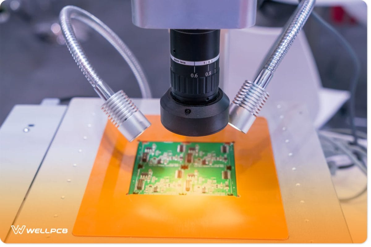
PCB Development
With this step, place your PCB as soon as possible into a bath made of sodium hydroxide with the sensitive part facing up. Then immediately, a blue-purple color appears and sometimes might be grey.
Gently shake the bath so that the design is visible at around 30” to 60”. After that, place the PCB in the water bath and wash it.
Engraving Your PCB
Here, the photosensitivity of your PCB is not minimal, and you can confidently switch the lights on. After this, carefully ensure that you place your PCB copper in an upward position into the FeCI3 acid bath while gently swirling it.
The solution needs to be in motion to enable the reaction to occur. At around 20’ to 40’ –depending on the water bath’s temperature, the copper’s surface area will dissolve. Such takes place immediately; remove your PCB, rinse it in a separate water bath, and then let it dry out.
Washing of your PCB
The remaining resin that was stuck onto the circuit needs some scrapping. But to easily do that, you will have to place the PCB slowly in an acetone bath, and if you are keen enough, you’ll notice the acetone turning to become yellow.
At around 10” to 20”, the remaining copper gets exposed. Now, gently place the PCB in the water and scrub it.
Tinning Your PCB
Tinning is optional, and you may choose to ignore it. Still, you should do it since it will come in handy, especially if you solder your components and avoid corrosion instances that may damage your PCB.
To do this, you will have to place the almost ready PCB into an empty bath while ensuring that you gently sprinkle a solution of tin-II chloride on it.
Are you done with the above step? If so, then you single-handedly made a presensitized PCB that is ready to be used.
Drill the PCB
It would help if you used a vertical drill in combination and a drill bit of 0.8mm to drill all the holes in your PCB. However, there are a few cases where you will find the 0.8mm drill somewhat not full enough compared to the components that need to go through.
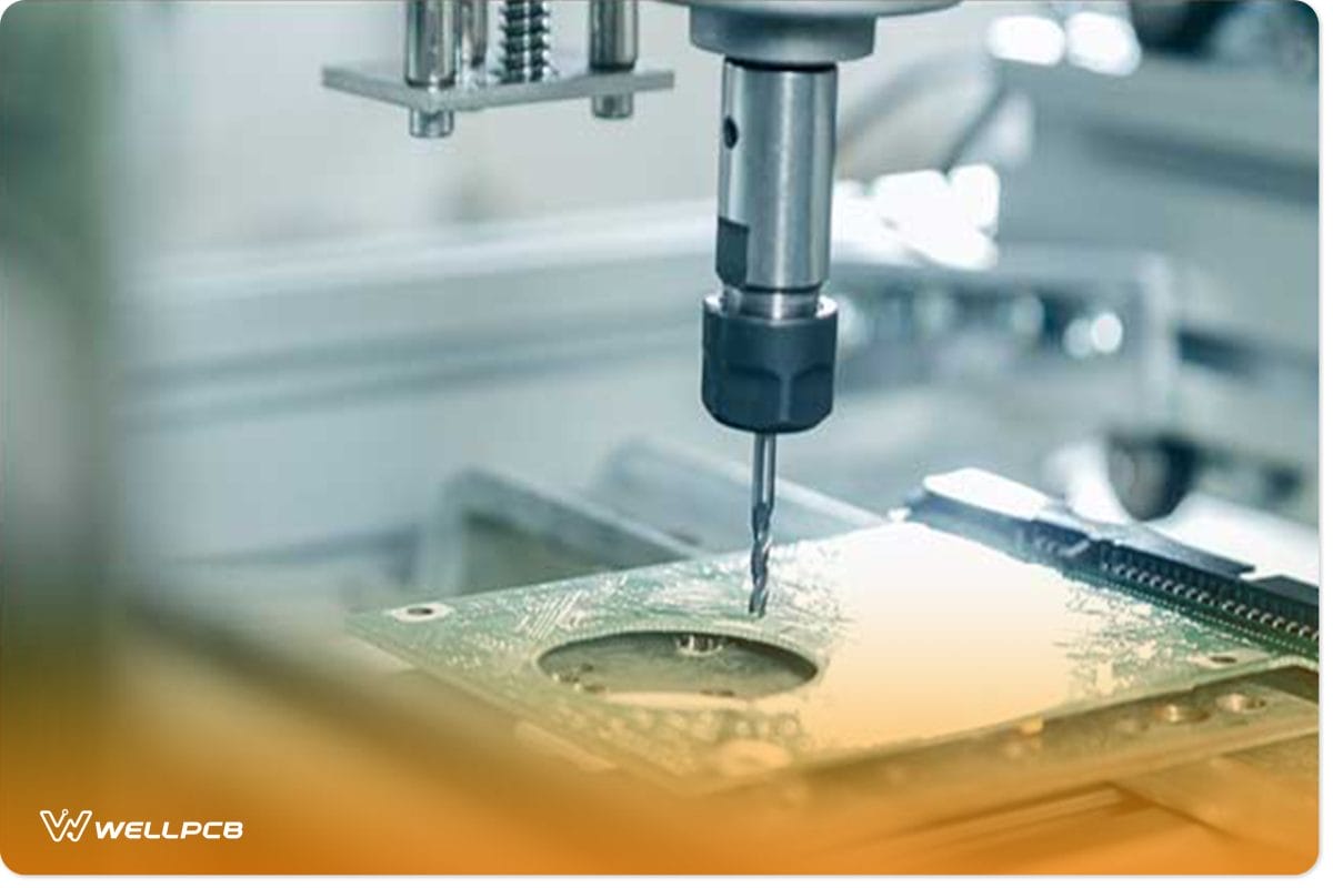
If you encounter the above scenario, don’t panic at all. Such cases are common. If the component gets too large to go through, a drill bit of 1.2mm comes in handy to widen the first hole in your PCB. Again, some caution is necessary here.
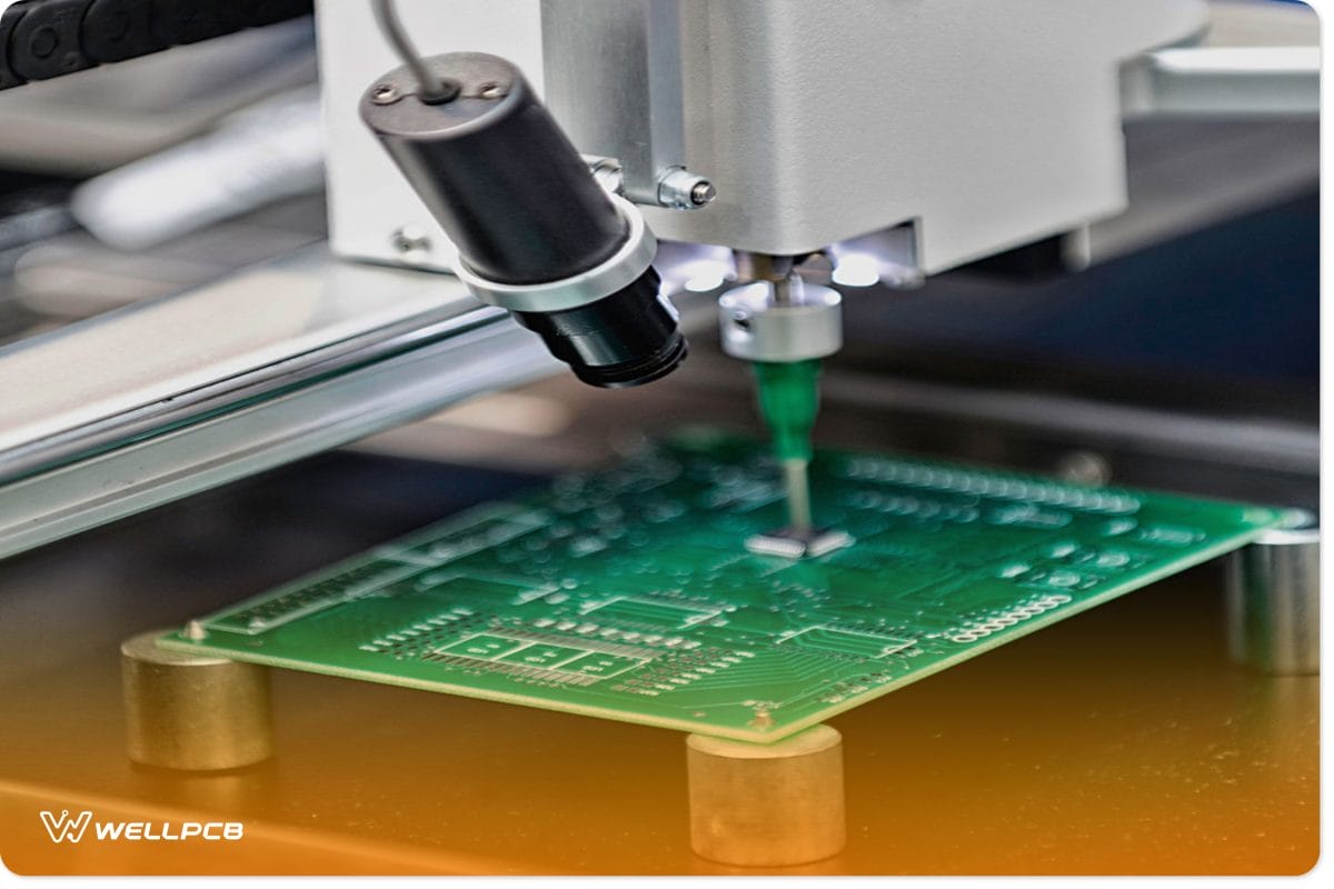
How to Etch Presensitized PCBs
PCB etching is one of the most vital steps involved in the chemical processing of subtractive PCBs. This process consists of the removal of copper to achieve the desired or required circuit patterns. When it comes to PCB etching, you should remove all the copper except the circuitry that the tin plating shields and which the application is crucial during previous treatment in PCB manufacture.
Etching presensitized PCBs can turn out to be one of the most complicated undertakings, but in the real sense, this is not a difficult task, as you may imagine. After gathering all the materials, you will print the layout and then begin by having your circuit layout printed. To ensure that everything comes out as desired, you may have to write the design in a transparent material such as acetate.
Printing the acetate needs to be done using a laser printer instead of an ordinary inkjet printer, which many people are fond of. The good thing about printed ink on acetate is that it will not stick and bring about undesired results.
Using a toner from laser printers well will still do the job. However, if you don’t have any laser printers available in your home, you can look for the nearest photocopier stand and inquire about a photocopy on acetate.
Locally etching solutions such as ferric chloride are in the form of a powder or solution. The developer comes in the form of a powder that you will have to dissolve using warm water, and here, you have a universal PCB developer! In case of dust, employ the same process with the developer, and upon completion, your board is now ready.
UV photo-resist Presensitized PCBs
The ultraviolet photoresist is one of the most critical features in dry fil development. That is a straightforward chemical reaction that is kick-started or initiated by the UV light, so it gets its name UV activated photoresist.
The whole process begins by coating the substrate using a light-sensitive organic material. A solvent commonly known as a developer is then carefully applied to the surface. After that, a patterned material is slowly and carefully applied to the surface to block light, a move that ensures that only the unmasked regions of the PCB have exposure to light.
In a positive photoresist event, a photosensitive material is degraded by light. The developer dissolves away the regions exposed to light, leaving behind a coating on the area that had the mask. However, in the event of a negative photoresist, the photosensitive material will be strengthened by light. The developer will dissolve away the regions not exposed to light, leaving behind a coating in areas where the mask had no reach.
Plenty of presensitized PCB and other dry film developers employ the same principle. The board is coated using a particular blue or similar shade pigment ink that is stable during storage in a dark room and positively reacts to an activator solution mixed with it when it experiences exposure to UV light. The reaction brings about a full settlement of the ink on the PCB that plays a photoresist’s role.
Advantages of Presensitized PCBs
Several advantages are associated with presensitized PCBs, which makes them the perfect choice for many manufacturers or producers of electronic instruments, equipment, and components everywhere. The advantages of pre-sensitized PCBs are as below.
Presensitized PCBs are compact and save a lot of wire. Presensitized PCBs are characteristic of interconnection between components through copper tracks instead of several cables that carry current. With presensitized PCBs, the interconnections are somewhat less bulky.
Presensitized PCBs are straightforward to repair if they malfunction or get spoilt. In damage, presensitized PCBs are very easy to check and subsequently replace specific failure components. The electronic components in pre-sensitized PCBs and their polarities are correctly designed and clearly labeled on the board.
Traditional PCBs take a lot of time when it comes to connecting their components. They save a lot of time, especially when it comes to assembling it. However, presensitized PCBs take much less time, which is why many people prefer them.
Plenty of pre-sensitized PCBs are immune to movement. If you happen to be keen enough, you will notice that most components in pre-sensitized PCBs have a firm grip on the board. Using the solder, which does not allow them to move regardless of the board’s movement, they are steady.
They are known to be very reliable as opposed to conventional PCBs. When it comes to reliability and performance, presensitized PCBs are known to offer some of the best results, which is why plenty of electrical manufacturers prefer using them instead of traditional PCBs.
Conclusion
Lately, there seems to be an overwhelming increase in the use of presensitized PCB. First, making these devices is not as complicated as it may sound, provided one carefully follows all the necessary steps from the beginning to the end. Besides design and the whole process of manufacturing presensitized PCBs, there are several advantages associated with presensitized PCBs; as mentioned earlier, so many electronic manufacturers worldwide prefer using them instead of conventional PCBs. Presensitized PCB can be a perfect trail board for experimenting based on low cost and few fabrication steps. We at WellPCB are very eager to work with you and get your Presensitized PCB order delivered!