Contents
1. What is a Barebone PCB?
Manufacturers design Barebone boards so PCB hobbyists like you can configure and populate them quickly.
Besides, Barebone PCBs offer hobbyists the flexibility of fitting them with parts that meet their demands.
Therefore, manufacturers should test the efficiency of these boards before releasing them to the market.
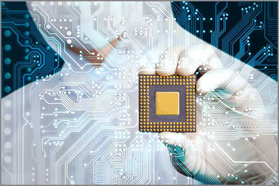
Barebone boards are the ideal examples of what precisely PCBs are. PCBs direct current on surfaces via copper pathways, meaning they influence electric paths in circuits.
It is important to note that circuit boards can be designed using various software, such as KiCad, Altium, Eagle, and others.
Such software will help you to output PCB design in different ways. The primary design methods you will probably encounter are Gerber and ODB++.
You can customize a PCB to meet your specific needs.
However, the main issue you will encounter in your PCB designing process is the prototype board turnaround time.
The whole manufacturing exercise and the shipping process will affect your turnaround time negatively.
There is a high chance that it will take weeks to a few months between when you make an order and when the manufacturer delivers it.
The long waiting makes recapitulating the circuit board design sluggish and frustrating.
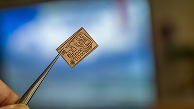
The best way to speed up your circuit board prototyping process is to use the Barebone PCB technique.
This is one of the quickest methods of creating quality and cost-effective boards.

2. How do I Use the Barebone Board?
First, arrange every component you need to run your PCB to achieve your desired functionality.
Choose and arrange the substitute components that will mthatmakey should make non-standard components.
Secondly, take a print of your schematic sketches and circuit board assembly drawings and examine them well. Ensure that you have not placed even a single component or solder wrongly.
Otherwise, you may need to re-work on your PCB, leading to a waste of time and resources.
Thirdly, place and solder all your capacitors and resistors on your PCB.
Remember to exercise extreme care when handling the polarity of your polar capacitors and Diodes.
You should solder your radial capacitors and through-hole parts from the lower side upwards.
Fourthly, mount and solder your microcontroller IC socket above the corresponding footprint.
Then, position and solder your programming headers and power source connector jacks.
After that, verify your soldered parts in line with the schematic and board assembly drawings. Also, remember to clean your board.
Lastly, program your microcontroller using a USB cable per your instruction manual.
It is also important to realize that you can program a Barebone PCB using either Arduino or Freeduino language.
A compiler consists of a microcontroller’s internal support and external peripherals, such as UARTs. Your Barebone PCB should have headers spaced 100 miles apart.

3. How to Solder Barebone Board
The Barebone board service from WellPCB is a good alternative for getting your circuit boards designed and delivered fast.
This will enable you to continue testing and rehearsing on your DIY project, avoiding delays between prototypes.
When you need to source one prototype PCB from other PCB makers, you can probably carry out more than two prototype design iterations.
The best thing about Barebone PCBs is that the speed does not increase the cost!
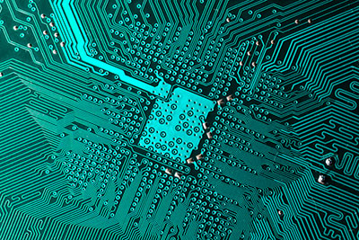
Notably, most circuit boards use solder masks to shield traces and negative spaces on the surfaces.
These masks prevent the formation of solder bridges between tightly spaced pads.
Solder masks can be made using substances that do not stick to solder.
The surface tension from the heated solder during the reflow process pulls the solder into the PCB pads.
However, since Barebone PCBs do not contain a solder mask, the solder tends to create bridges between the PCB pads.
This becomes a significant problem since these bridges can create short circuits, malfunction your PCB, or even damage the entire device.
Thus, when soldering a Barebone PCB, ensure you carefully distribute solder paste evenly to avoid applying too much, creating solder bridges.
Alternatively, you can hand-solder your board, assuming it works well with your design.
When working with Barebone boards, you should always spare some time to test your board before powering it.
3.1 How to Minimize the PCB Prototyping Time
The PCB prototype production can consume much time, mainly the designing and shipping.
As mentioned earlier, the time between making an order and receiving it can take several weeks to months. You can use the Barebone PCB technique to accelerate this time frame.
Barebone boards have a turnaround time of 24 hours.
Including about four days of shipping your products implies you can make a prototype circuit board in less than one week of ordering.
Our Barebone PCB technology can create circuit boards within hours by eliminating various standard production steps employed in the standard circuit board manufacturing process.
Barebone PCBs do not have solder masks and silkscreen.
Additionally, the Barebone technique does not permit internal cut-outs.
By eliminating some production steps, you will be able to produce Barebone boards quickly.
Consequently, this will enable you to iterate your project faster.
Nevertheless, it will be difficult for you to solder on the PCB since it lacks a solder mask.

4. The Benefits of Barebone PCB
As highlighted in the introduction, nowadays, manufacturers are continually miniaturizing electronics.
As inventors develop new technologies, engineers search for innovative ways to make their offerings smaller and more efficient.
However, many hobbyists ask themselves whether making electronic products smaller has any other benefit besides saving Space.
Miniaturizing parts and using smaller boards have numerous spaces that can significantly benefit you.
Below are the main benefits of Barebone PCB technology.
4.1 Barebone PCB– Lower costs
By miniaturizing parts and embracing smaller PCBs, the Barebone technique minimizes the materials you need to make PCBs.
Because of this, leveraging miniaturized PCBs can decrease your overall production expenses.
While you may spend more researching and developing a custom miniaturized technology, you will enjoy more long-term cost-saving advantages of using fewer production materials.
In the long run, you will save on transport expenses.
Still, if you have fewer shipping materials, you can ferry more at the same or less price.
4.2 Barebone PCB– Saves SpaceSpace
Shorter boards are ideal for making PCBs for smaller gadgets, such as smartphones and tablets.
For example, you need to mount the PCB and fix numerous other parts in smartphones.
Hence, the more room you create by applying small boards, the more space Space will have to accommodate other components.
4.3 BareSpacePCB– More Eco-friendly
Since the Barebone PCB technique eliminates some manufacturing steps, you will require fewer materials.
When you apply fewer materials, you will eventually emit fewer waste products to the environment.
While most PCB components can be recycled, miniaturized boards require even minimal materials; therefore, they will require less recycling.
5. Barebone Board Design Limits
The first restriction point you should consider is that a design should not integrate internal cut-outs. This implies that you should not request a design with parts routed outside the PCB apart from holes.
Secondly, your design should be bigger than one inch in every measurement.
If your design is below one inch in any measurement, the Barebone board design will automatically enlarge your PCB outline to a dimension of at least one inch.
6. Making Gerber Files for Barebone PCB
When you have a complete design that aligns with the Barebone guidelines, the other step you should make is generating Gerber templates from the circuit board design.
It is important to note that Gerber files are the typical method engineers use to represent circuit board design for production purposes.
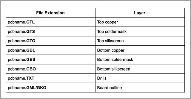
Most Barebone circuit boards apply only a few layers: upper copper, lower copper, drills, and board outline.
However, in Autodesk Eagle software, the CAM processor you will employ to create Gerber files automatically creates all the files.
With this in mind, Autodesk Eagle is the best software for generating Gerber files, especially for beginners.
Conclusion
The Barebone board service from WellPCB is a good alternative for getting your circuit boards designed and delivered fast.
This will enable you to continue testing and rehearsing on your DIY project, avoiding delays between prototypes.
When you need to source one prototype PCB from other PCB makers, you can probably carry out more than two prototype design iterations.
The best thing about Barebone PCBs is that the speed does not increase the cost!
Generally, Barebone PCBs are cost-effective and miniaturized alternatives to Arduino PCBs.
With the continuous technological inventions and the preference for more portable electronic devices, PCB manufacturers are shifting to smaller Barebone PCBs.
WellPCB has a wealth of experience in PCB designing.
If you need printed circuit board services, kindly contact us for a quick turnaround.
We are at your service!