In case you didn’t know, about half of all designed PCBs (globally) is faulty. They never get through the PCB manufacturing phase. And 30% of those that enter the market fail after their release.
Why do so many PCBs fail in their production?
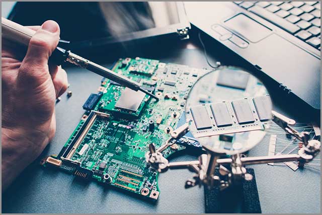
There are simple, minute details that we ignore during the circuit board manufacturing process. This ignorance of more information turns out to be too costly.
Contents
A Billion-Dollar Mistakes
About five years ago, General Motors made a $4.1billion mistake. One of their model cars is the ignition key had a PCB design flaw that was overlooked by its engineers.
Thanks to the PCB mistake, General Motors had to recall all its model cars and compensate its buyers using a few billions of dollars. It also had to hire some high-end lawyers to handle numerous lawsuits.
Think about it: here was a perfectly functional million-dollar car, let down by its ignition key! Just an ignition key! Gulp. What a waste?
Was The GM is an isolated case? No. A few years later, Samsung made its historic $5.3B worth PCB design mistake. It was followed by McDonald’s with their fitness device PCB design flaw that cost them $33 million.
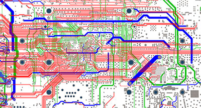
In this edition, we will look into the seven common areas to note during PCB manufacturing.
Take Note of the Starved Thermals
Thermals are tiny traces around pads that interconnect pads with the plane. As their name suggests, their central role revolves around heat circulation. Their primary design purpose is to enable the heat sink to efficiently dissipate heat from the heat sink to the heat sink. Thermals are also critical during soldering due to the high amount of heat used in soldering.
Then again, a few people have an interest in the pads during WellPCB. We will provide you with one-stop service and high-quality products. You can send us the documents you need to make and get a quote immediately! What are we waiting for? We have ten years of PCB manufacturing. As a result, you may (sometimes) ignore the significance of the thermal interconnections. By doing so, you will create a void between the pads and the plane. The emptiness then creates an incomplete thermal interconnection.
We refer to such faults as “thermally starved” interconnections.
Thermal starving is the root cause of heat-related complications in most PCBs. It lowers the rate of heat transfer when your circuit is under heat stress or during soldering.
As a result of reduced heat circulation, a thermal pad could solder oddly or take a longer time to reflow. This unnecessary delay will eventually lower the assembling process or produce gadgets that are in danger of overheating during operation.
Thermal Starving can arise during either the PCB designing or the WellPCB. We will provide you with one-stop service and high-quality products. You can send us the documents you need to make and get a quote immediately! What are we waiting for? We have ten years of PCB manufacturing phase.
Usual PCB designing tools won’t identify starved thermals. However, an experienced correct PCB service provider. Thankfully, there are various PCB manufacturing company can help you to identify and rectify such faults.
Acid Traps are Avoidable
An “acid trap” is a term we use to refer to the acute angles in a circuit design. We use this term because these angles trap unnecessarily excessive acid during the etching process. The trapped acid builds up and stays on the edge of the bend for an extended period than it is required.
This stagnant acid can eat up the material making the circuit than it was required. As a result of the acid corrosion, parts of your PCB connections would end up being either weak or defective. Such a fault could become fatal on life-supporting devices.
Most acid traps occur during manufacturing. As a PCB designer, acid traps are often not your fault. You don’t create them, except that you do design them. And that should worry you because even though you aren’t directly responsible, you do hold a higher power of minimizing their occurrence.
Your PCB is your business. Thus, most PCB designers hare trained to avoid acid traps. However, you may, at times, make a blunder. Especially when using those simple PCB designing applications with “auto-generate” capabilities.
If you always double-check your PCB design, you will possibly eliminate acid traps. But in case you missed to fix them, we could help you out with the aid of our DFM tools before we manufacture them for you.

Silvers
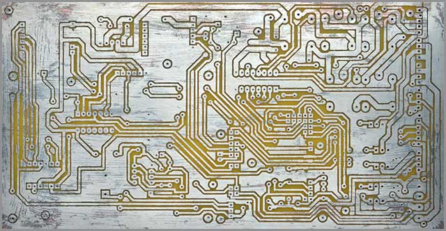
Silvers are thin wedges of copper or solder mask produced during the etching process of PCB manufacturing. Usually, silvers occur when long and thin strips of copper or solder are etched away and dispatched before they fully dissolve.
These dispatched silvers could dissolve into a chemical bath and later be added unintentionally onto a different board. This act could result in the creation of unintended connections.
Sometimes, silvers can arise from cutting a PCB section either too narrowly or too intensely. Even though intended to stay on the board, such silvers are prone to detach either slightly or entirely. Such incidents create unintended circuit breaks that could renter an entire circuit useless. Silvers are also hard to identify and rectify.
You can avoid silvers during PCB designing by designing PCBs with minimum widths.

Designing With Sufficient Plate-To-Edge Clearance
Copper is the most widely used PCB conducting progressive metal. It is preferred over other metals owing to its high conductivity and its ability to remain inert when exposed to most reactants. On the flip side, copper is reasonably soft and corrosive. We plate copper with other insulating materials during PCB manufacturing to minimize the risk of corrosion.
Even so, when trimming PCBs, sometimes the protruding copper layers and connections close to the surface can get exposed. This exposure can cause considerable risk to the stability of your PCB.
First, the exposed copper connection can connect accidentally with a different component on the same board, short-circuiting your board’s components. Alternatively, the exposed copper section is at the risk of being corroded. On the chance that the two fail, then the exposed copper endangers the handlers of your PCB from receiving an electrical shock.
It is necessary to design your PCB while retaining proper distance between the copper plate and the edge of the board to avoid such mistakes. This distance is sometimes known as the “copper-to-edge” or “plate-to-edge.” A DFM inspection for the standards before manufacturing can establish such design flaws.
Having Voids When Plating
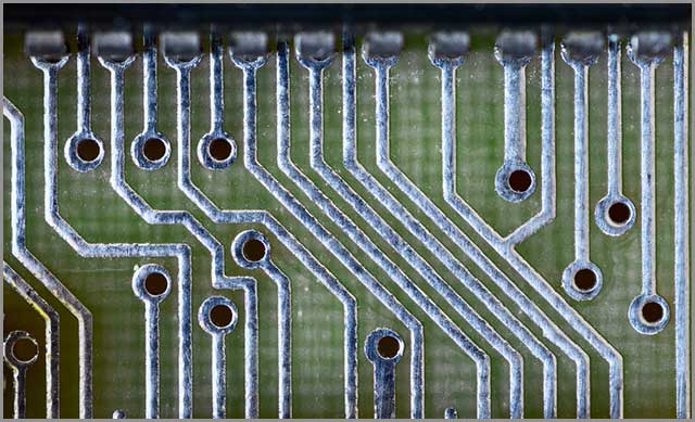
During the process of creating vias, it is necessary to create room for through-hole vias — these holes aid in interconnecting one side of a PCB to the other.
When creating through-hole vias, the fabricator drills the holes by cutting through all the sections of a PCB — for copper plating film holes separated. This act deposits a thin layer of non-conducting copper material in a process known as a deposition. A few more copper layers get added to complete the circulation.
At times, the deposition process is faulty. It is thus possible to plate voids or air bubbles. This act results in unexpected circuit breaks that are internal and hard to detect or repair.
Such problems arise during manufacturing. They will then cascade to the manufacturing stage. It is, therefore, necessary to choose an established PCB manufacturer with adequate tools and personnel to detect such defects.
Electromagnetic Complications
Electromagnetic Compatibility (EMC) and Electromagnetic Interference (EMI) are two main challenges to reliable PCB production. EMC is concerned with the generation, propagation, and reception of electromagnetic energy, while EMI is concerned with EMC’s side effects.
Uncontrolled EMI may lead to defective PCBs. To newbie PCB designers, distinguishing between the two can be a daunting task. But there are a few common design considerations you can employ, like minimizing 90-degree angle placement for components and increasing the ground area. If you are uncertain, it is advisable to use shielded cables to reduce EMI.
Avoiding DFM
DFM or “Design for Manufacturability” is a term we use to denote a process of inspecting circuit boards for standards compliance. During the process of DFM, we analyze the PCB design for possible complications during design or assembly. It mainly tests whether the PCB will reach its set goals.
Besides testing functionality, DFM also tests to see how a PCB will break. DFM assesses a PCB from the worst possible occurrence. It can evaluate the topology of the PCB and identify most design flaws that are usually ignored by typical CAD software applications. It checks and compares design defects with other existing database checks drawn from a vast pool of PCB considerations. DFM checks are the final checks before mass PCB production.
Take Note
When you keep changing your PCB manufacturer, your PCB prototype might not function as your final production.
PCB manufacturers play a significant role in determining the PCB quality produced. The manufacturer may alter your original PCB design to conform to a standard before manufacturing it. These changes will remain with your manufacturer.
Thus, when you change your manufacturer, these changes vanish. It is, therefore, recommendable to order your PCBs from a single, trusted PCB manufacturing company.
Summary
If you are on the verge of PCB production, we can help you to get it out flawlessly. Our team of professionals is ever willing to respond to your queries inquiries when you are stuck. As reputable manufacturers, we have invested in having cutting edge technology when performing DFM checks to ensure quality production of our PCBs.
Feel free to reach out to us today, and we could help you to get it done.


