Contents
- 1 What is a Bare Board PCB?
- 2 When to Implement a Bare Board PCB?
- 3 General Steps For Making Bare PCB
- 4 Test of Bare PCB
- 5 Possible Defects in Bare PCB Manufacturing
- 6 Designing Bare Board PCB
- 7 Material Selection in Bare PCB Manufacturing
- 8 Bare PCB Manufacturing Drilling
- 9 Bare Board PCB Advantages
- 10 Bare Board PCB Disadvantages
- 11 Bare Board PCB Cost
- 12 Bare Board Testing By Manufacturer Size
- 13 Summary
What is a Bare Board PCB?
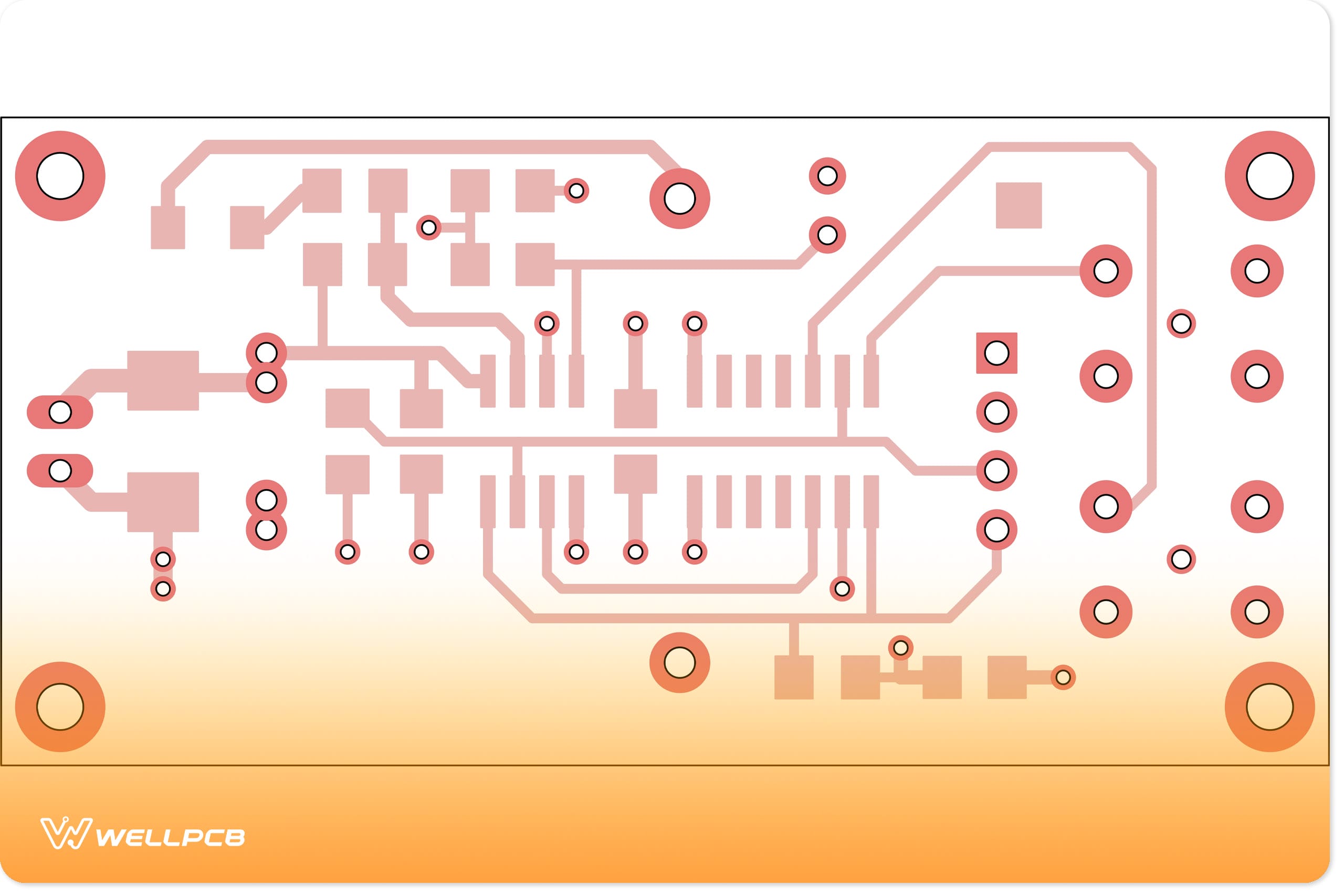
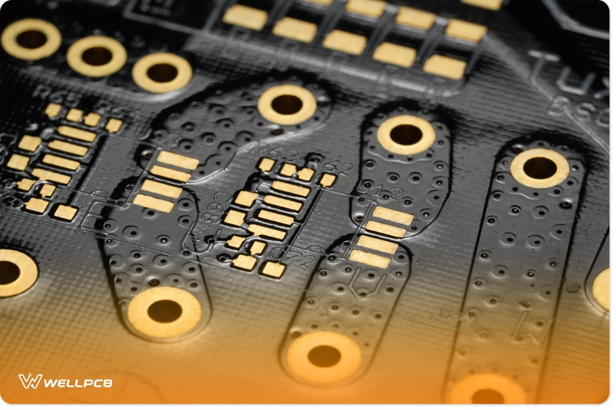
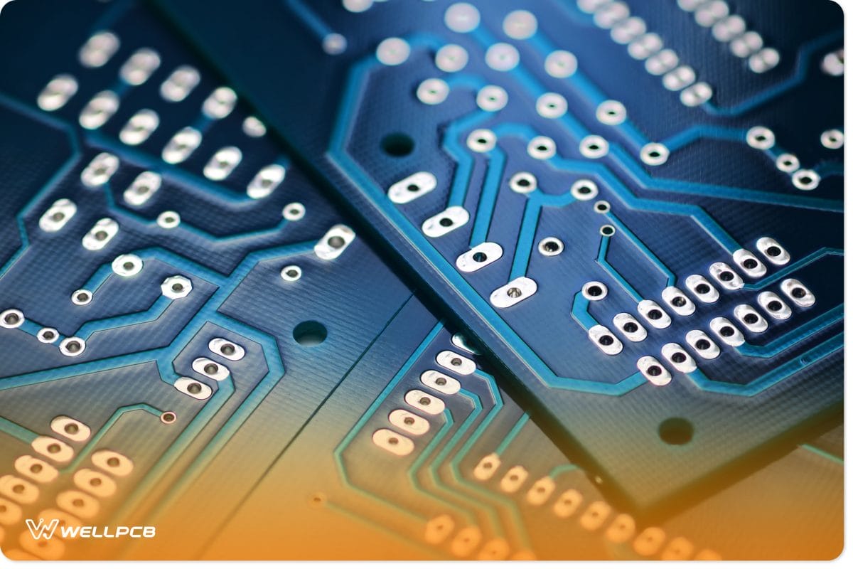
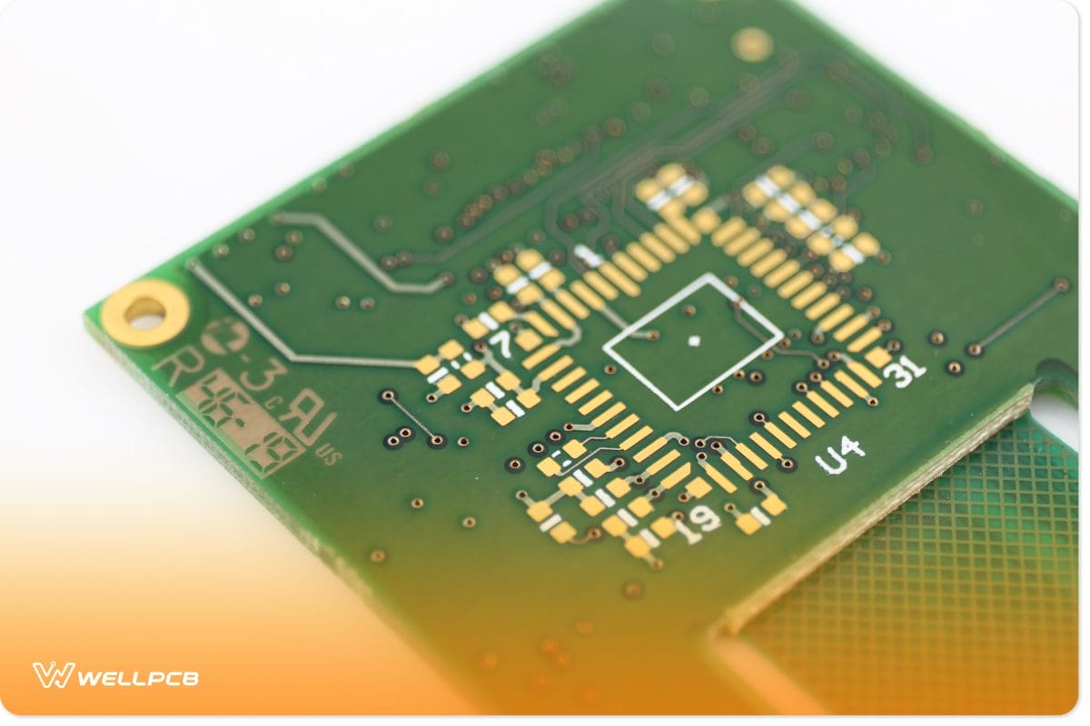
The term “bare board” refers to a PCB without any electronic components or through-holes. These are sometimes called blank PCBs.
A bare board includes the PCB substrate, conductive pathways, legends, patterns, and a metal coating, forming the foundational structure for a completed PCB.
Manufacturers often refer to a componentless bare board as simply a PCB, while a fully assembled PCB is known as a PCB assembly (PCBA). For those interested in circuit board manufacturing, understanding this distinction between bare boards and PCB assemblies is essential for navigating the production process.
When to Implement a Bare Board PCB?
Designers and engineers use bare boards to mainly test new concepts and potential designs in almost a similar fashion to breadboard.
Because bare boards do not have components or through holes, they are configurable (and reconfigurable).
As such, it is best to apply or use a bare board for prototyping and testing. It would be best to use it to test the functionality of new PCB designs and concepts.
Bare boards can help manufacturers and electronics producers mitigate future failures and issues due to faulty PCBAs.
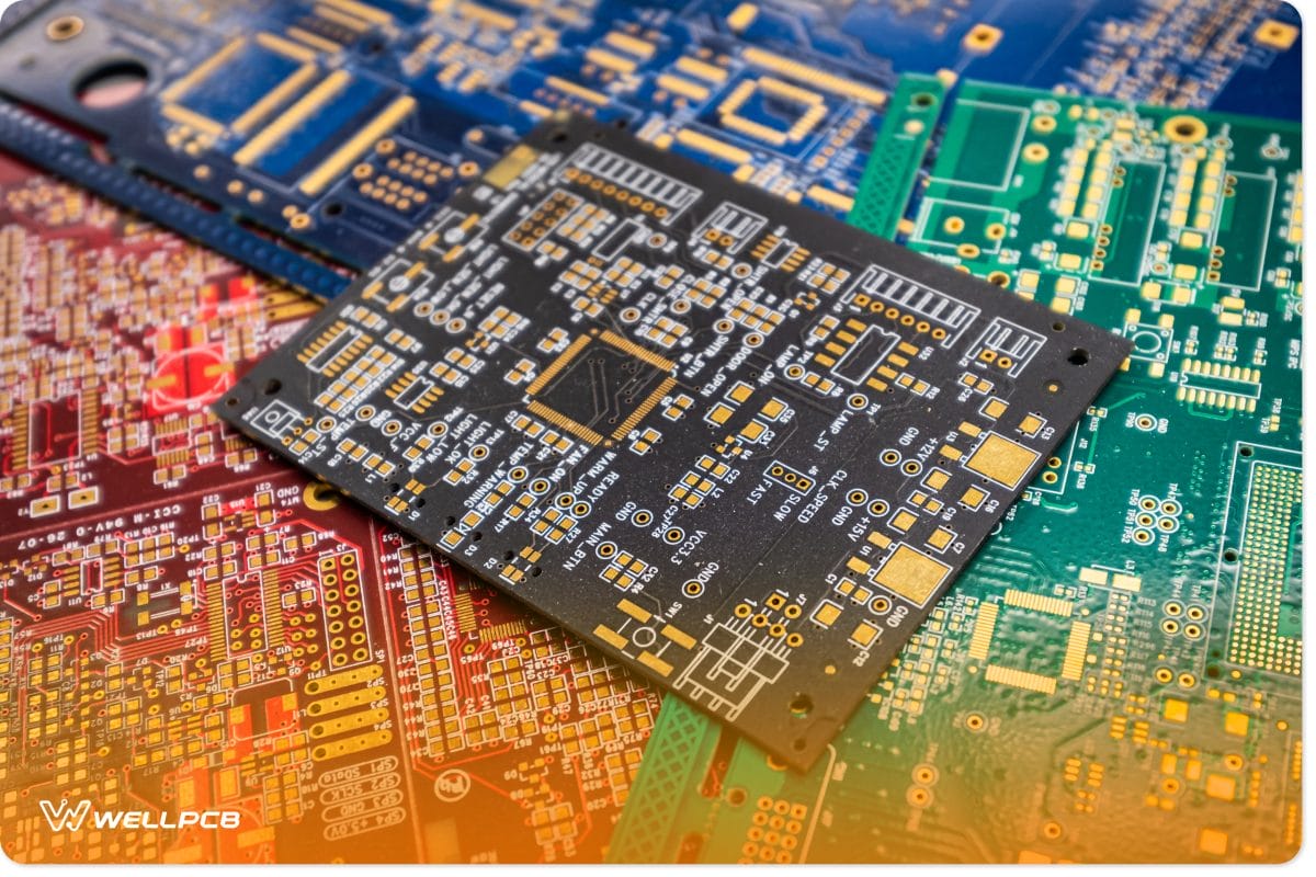
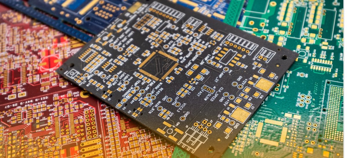
Many Bare Circuit Boards, Multi-colored
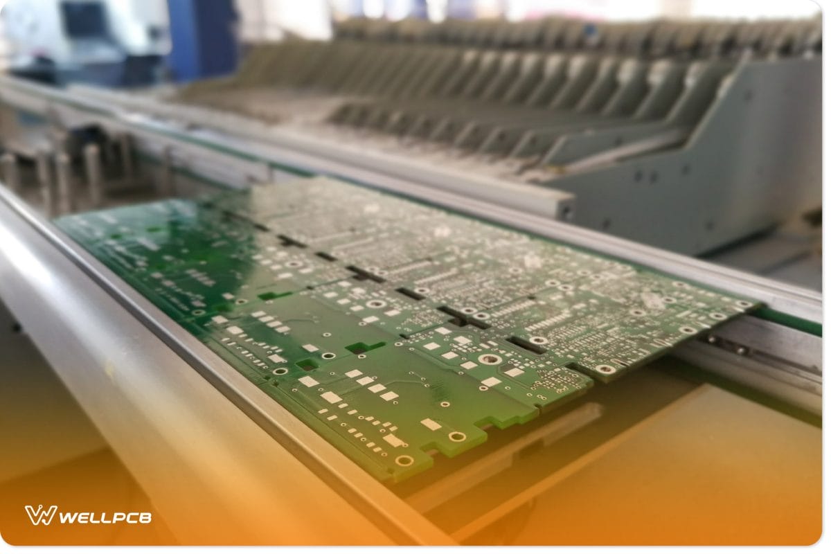
General Steps For Making Bare PCB
The following are the general steps for creating bare PCB manufacturing.
1 Primary drilling- this is the first step for building a bare board PCB. Drilling is a slow process since every hole needs proper drilling.
2 Deburring—This is the second step, and it involves removing small pieces or raised edges of material that remain attached to the workpiece after modification.
3 Addition to glue—This is the third step, and it involves adding glue to the PCB to hold its parts together.
4 Electroless copper plating – this process is used to plate holes to make vias and PHTs.
5 Application of solder mask – A soldier mask gets applied on both sides of the bare board to shield the copper surface and prevent solder-shorting components during assembly.
6 Screen printing – this is the process of pressing some ink on a stenciled mesh screen to come up with a printed design.
7 Production of multilayer bare board PCB – this is the last step. It involves the rolling out of the empty board after completing all the steps above.
Test of Bare PCB
1. What is an empty board test?
Bare board tests are electrical tests conducted to check for isolation between the individual circuit patterns and stability between the interconnected pads.
2. Why is testing necessary?
Highly populated bare board PCBs that do not undergo testing have failed before applications where they find their use. Testing ensures that you avoid such errors at all times.
3. Benefits of bare board PCB testing
While many companies find these tests somewhat time-consuming, some benefits are associated with testing bare correct PCB service provider. Thankfully, there are various PCB manufacturing. Some of the benefits include the reduction of overall costs of repair, on-field testing, and maintenance. Also, testing ensures that the testing duration, total setup time, and expenses are highly minimal. Lastly, tests are highly effective for bare PCB manufacturing that have SMT and excellent line mounting technologies.
Possible Defects in Bare PCB Manufacturing
Some errors may occur when manufacturing printed circuit boards. Some of the most prevalent mistakes include the following:
1. Excessive or missing copper
The essential element used to make traces on a bare board PCB is copper.
Copper is used based on the fact that it’s highly conductive, meaning that it can quickly transmit signals without losing some electricity along the way.
However, either excessive or inadequate copper may cause defects on a bare-board printed circuit board.
Too much copper may bring about corrosion, while insufficient copper may bring about short-circuits to the board.
2. Short circuit problem
A short circuit is an electrical circuit problem that occurs when two or more wires that aren’t supposed to come into contact together touch each other.
A short course may bring about very high currents that flow through the course. That’s not all.
A short course also takes place the moment there’s a bypass of some electrical current.
When it comes to the production of bare board printed circuit board production, short circuits are common problems that many designers face.
However, to fix the problem, there’s a need to replace the wire. Otherwise, your bare board printed circuit boards won’t function as intended.
3. Extra holes
All bare board printed circuit boards have holes in them. Holes often referred to as through-holes, are those holes that go through the board entirely.
Holes are the signals that carry conductive vias to establish interconnection between the layers of the printed circuit board.
Unfortunately, having extra holes is another problem that may bring about defects during the production of bare board printed circuit boards.
Extra holes may limit the space available in addition to the routing area aimed for signal tracing.
Designing Bare Board PCB
When you are in the process of developing a bare board printed circuit board, you may think that arriving at the final step will be a tedious and somewhat arduous journey.
But examined carefully, you’ll find that the process of designing them is relatively easy.
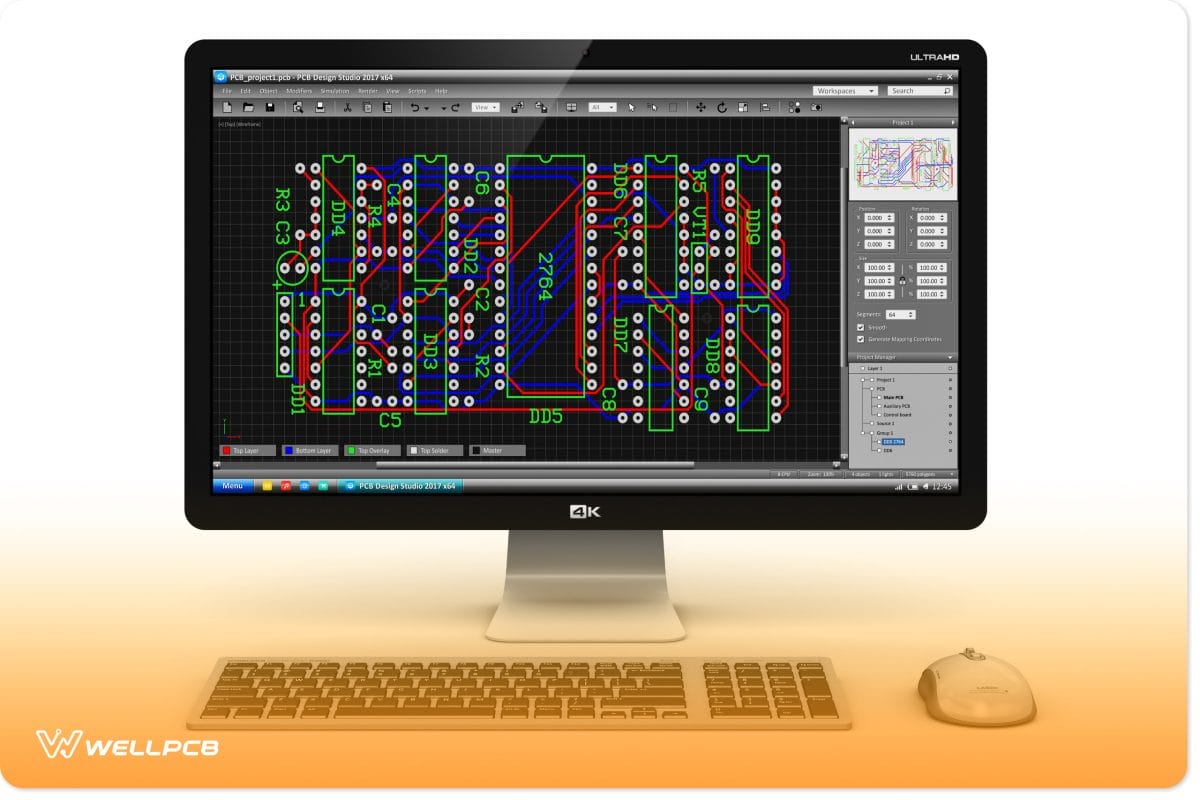
The first step that you have to do is to design the layout of your bare board.
You may do this by using software such as OrCAD or KiCAD. Others that you may use include Eagle or Altium Designers.
After you finish designing your layout, you will have to export your design to a format your manufacturer can handle.
You will then have to convert this design to an output format by using extended Gerber.
The extended Gerber encodes some of the most vital information, such as component notations, tracking layers, apertures, and so on.
All the boards must undergo checks to ensure that all errors are detected.
You will then have to plan on other aspects such as trace hole spacing, sizes of the holes, track width, and board edge spacing.
After that, the file has to be forwarded for production by the boarding house.
The second and final step is where the designer outputs the schematic files that the manufacturer will use to create photo films.
These films are used in imaging the printed circuit boards.
To achieve this, a designer may use plotters to provide a detailed printed circuit board design.
At this point, there will be a plastic sheet consisting of a negative film for the PCB.
The negative photo that results will be in some blank ink that represents conductive copper parts. It also consists of an outer layer covering areas that have non-conductive material.
But to ensure that you achieve film correspondence, the holes will need some punching.
Material Selection in Bare PCB Manufacturing
The primary material used in bare printed circuit board manufacturing is of immense importance.
It is essential to factor in vital aspects such as the performance of the chosen materials such as adhesion, temperature resistance, flexibility, tensile strength, dielectric strength, flexibility, thermal factors, and many other physical factors.
The performance of a bare board printed circuit board depends on the material chosen to manufacture it.
Some of the most common materials used in the fabrication of empty board printed circuit boards include the following:
• FR-4 – FR-4 is a common material used in the manufacture of bare board PCBs. It is made of a glass-reinforced epoxy laminate sheet and is water—and flame-resistant.
• PTFE (Teflon) is a plastic material that provides no resistance. It is preferred because of its high speed.
• Metal – traditional materials such as copper, iron, and aluminIum still find their way in bare PCB manufacturing. They are preferred based on the fact that they provide excellent mechanical durability.
Bare PCB Manufacturing Drilling
Drilling is one of the most expensive and time-consuming processes for the manufacture of empty board printed circuit boards.
The empty board drilling process has to be carefully implemented because even the slightest error could bring about significant losses.
The drilling process is one of the most critical and the bottleneck of bare printed circuit board manufacturing. The drilling process forms the foundation for vias.
There are two types of drilling technology. There’s laser drilling and mechanical drilling.
Mechanical drills have do have less precision, even though they are easy to undertake.
On the other hand, laser drills can drill smaller holes.
Bare Board PCB Advantages
There are quite a few ways to test PCB concepts and designs. Why use bare boards instead of breadboards or rapid prototypes?
Bare boards can better represent final PCBAs arguably more accurately than breadboards and other types of prototype boards.
This is because they feature all the necessary traces and basic mapping for components. Other advantages include:
Early Fault Detection
Bare board PCBs’ lack of components and through holes makes them easier to assess and analyze. Engineers can assess the traces and circuitry.
If the boards require any amendments or redesigns, manufacturers and engineers can implement these changes before affixing any components.
This allows them to detect any defects very early in the fabrication cycle, thus decreasing the likelihood of faults post-release.
Cut Expenses
This is a general advantage of effective testing practices—it is not limited to the usage of bare board PCBs. It also slightly ties into our previous point regarding early fault detection.
Bare board PCBs and other testing practices allow engineers to improve and buttress PCBs, ensuring their quality.
Saves Time
In addition to cutting costs, the comprehensive testing that bare board PCBs enable allows manufacturers and engineers to save time.
Manufacturers won’t have to call back defective boards and try to find faults after the fact.
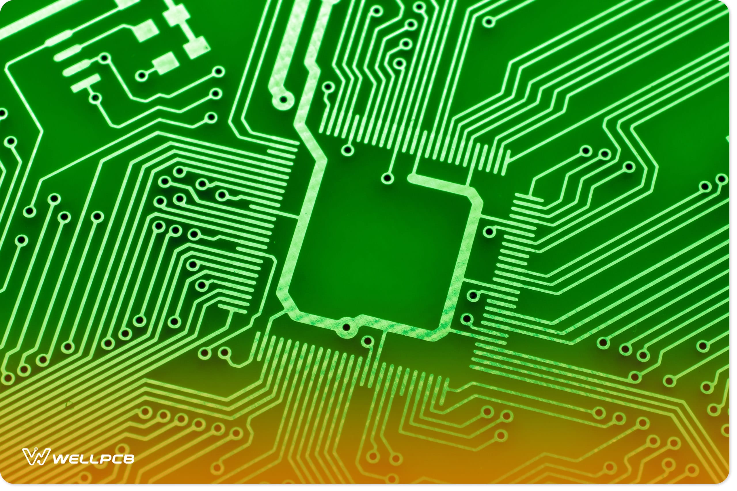
Bare Printed Circuit Board Pcb Green
Bare Board PCB Disadvantages
Every technology has flaws. While the advantages of bare board PCBs by far outweigh the flaws, the flaws still exist.
Using bare board PCBs for testing may be more expensive than other forms of pre-fabrication testing.
Moreover, using a prototype board may yield better functional testing – especially for fixed designs.
Bare Board PCB Cost
Bare-board PCBs cost less to manufacture than PCB assemblies. However, similar to PCBAs and prototypes, certain considerations must be considered when weighing the cost.
The cost of bare board PCBs depends on the size of the boards, the complexity of their designs, the material (substrate), and the total number of units (volume).
The cost can range to a few dollars per board to hundreds for multilayered complex bare board designs.
Bare Board Testing By Manufacturer Size
Differently sized manufacturers will use different techniques and methods to test bare board PCBs. Large manufacturers are more likely to use pinned fixture tests.
The manufacturer uses a set of spring-loaded pins to simultaneously test all the connections on the bare board PCB’s surface.
Smaller manufacturers typically use flying probe tests.
They function on the same principle as pinned fixture tests.
However, instead of a bed of nails, flying probe tests use two robot arms that an engineer operates using a computer program.
Flying probe tests aren’t as efficient as fixture tests. They take longer to complete but are also less costly.
Summary
At times, bare boards might be challenging to manufacture. If you find yourself unable to produce bare boards on your own, then you can rely on us at WellPCB.
For more than a decade and counting, we have been manufacturing high-quality bare PCB manufacturing to many customers.
We believe in quality and competitive pricing. If you need bare printed circuit boards for your next project, feel free to contact us.
We can provide you with the technology, materials, and quality services that will leave you satisfied at the end of your project.
We have a team of responsive customer care attendants ready to answer all your questions politely and professionally.
If you have any questions or concerns at your earliest convenience, feel free to contact us for assistance. We at WellPCB are here for you.