Contents
- 1 PCB Etching
- 2 Etching Types
- 3 PCB Etching Kit
- 4 PCB Etching Solution
- 5 PCB Etching Process
- 6 DIY PCB Etching
- 7 Laser PCB Etching Process
- 8 PCB Etching Machine
- 9 PCB Etching Process Display
- 10 What Can Go Wrong With PCB Etching?
- 11 How Long Does It Take To Etch A PCB?
- 12 What Should You Use For PCB Etching?
- 13 Conclusion
PCB Etching
What is PCB etching?
The PCB etching merely is defined as the selective removal of material from the surface of the Printed Circuit Board with the aid of the chemical action of an etching agent. Etching usually entails the removal of copper areas that are not needed on the completed Printed Circuit Board. The process of etching can be carried out by placing a cover that can shield the parts of the laminate and thereby excluding the copper layer. The PCB Etching is an easy and economical procedure that can be carried out at home or in the lab.
PCB etching Pen
The PCB Etching Pen is more like a water-proof pen enclosing permanent ink. The ink contained in the PBC etching pen has properties that can resist etching. The pen has a nylon tip that enables fast manufacturing of the printed circuit boards. An example is its use on Copper printed circuit board; Circuits can be drawn on plain copper laminate and then etched in Ferric Chloride or etchant solutions, this is allowed to dry for few minutes, then immerse the board in etching fluid until you confirm that the copper is dissolved. After the etching process, the ink can be evacuated with the aid of cleaning fluid or a Printed Circuit Board Cleaner. After this processes have been successfully carried out, then the circuit board is ready to be drilled and assembled.

PCB etching acid
The PCB etching chemicals used industrially
Here in this section, wne would go through

Copper etching PCB
To get rid of undesired copper from copper clad substrates to form electronic circuits, two methods are discussed. They include;
Mechanical etching: in mechanical etching, a special cutter and a machine tool are used to get rid of a narrow strip of copper from the boundary of each pad and trace. In doing this, the circuit elements are electrically separated from the rest of the foil.
Chemical etching: chemical etching depends on the activities of a corrosive fluid to chemically disintegrate away undesired copper to clarify the desired circuit.
In this process of chemical etching, etching is generally done by full immersion of the board in the chemical; an etching resist used to protect the desired copper from the etchant.
Etching Types

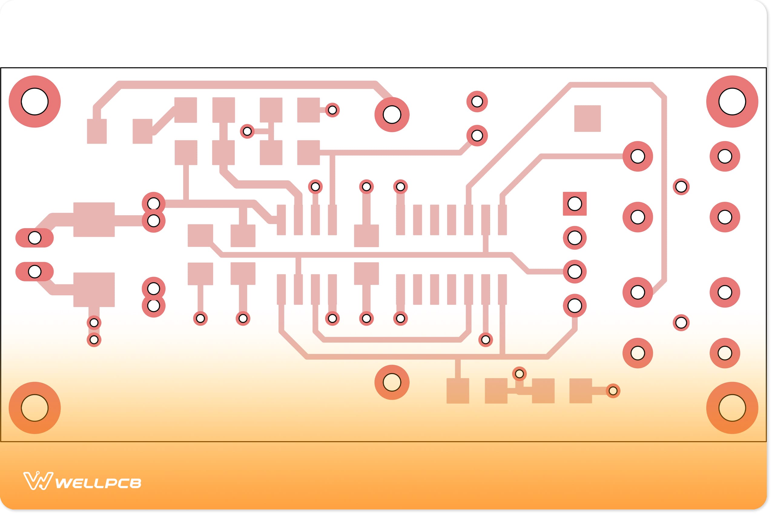
Circuit before and after etching.
Take a look at the two different etching types in the PCB world. Both of them, dry and wet, use their process to create the right design on the board.
Dry Etching
You can rely on one of these two techniques to etch your printed circuit board. This type is more physical and clean than the other.
Laser
With this method, a computer-controlled powerful laser hits the PCB to remove copper and produce the circuit design. It’s a precise way to get the etch job done that won’t put your circuit board through mechanical stress. That way, you won’t deform the PCB as much.
Plasma
If you pick this type, plasma gas ions will target your PCB to ablate the copper. And it’s perfect if your circuit layout has greater details.
Many have turned to plasma because it doesn’t harm the vias as much and soaks up any solvents. However, you’ll need to be aware that this costs more money.
Wet Etching

A PCB that will have acid etching done.
Doing wet etching is the other way to take on this job. Each of these has to do with subjecting your PCB to a chemical solvent that forms the circuit’s pattern.
Alkaline
People use the alkaline one to etch the outermost layers of a circuit board. The PCB goes in a high-pressure chamber that sprays it with a chemical like sodium hydroxide. Doing so forms the circuit pattern you want on it.
Acidic
By using the acidic approach, a PCB’s innermost layers will get etched. Some may try this one because it won’t affect the parts. And the etched area under the tin layer doesn’t laterally erode too much.
PCB Etching Kit
The PCB etching kit comprises of different tools (combining matching materials with chemicals) that can be utilized in fabricating the printed circuit board from the scratch to the completion.
Now that you are familiar with the fundamentals of PCB design, it is often difficult for starters to choose suitable etching tools to fabricate their printed circuit board.
The only difference that can be made with the tools is selecting the best out of various available ones in the market.
After merging the tools and chemicals, it might still not yield a perfect result, and this is because the chemicals might not be in a balanced ratio, or the materials may not fit together perfectly.
It is hard to get the small drill bits for making the PCB holes, and due to this reason, the PCB etching kit packages the required drill bits.
Included in some starter’s PCB etching kit is a small dc driller motor that can be used in making the holes.
The material’s quantity ratio must be carefully selected to avoid needless components. As time goes on, the skills of PCB fabrication can be perfected.

PCB Etching Solution
When we refer to the cheapest and readily available solution for PCB etching, we are referring to ferric chloride. Ferric chloride is available as a liquid or in concentrated form, which must then be diluted. When this solution is used, immerse your PCB board in the liquid, wait for a little while, and check to see how far it has gone.
Though heating the liquid can be very helpful, it is not necessarily required. Ferric chloride is cheap, but it cannot be used over and over, and it is not environmentally friendly. Therefore, after use, it is essential to dispose of it properly at a waste site.
Another solution is the Ammonium persulphate which is available for copper etching PBC, and it is often used in etching circuit boards. Ammonium persulphate is a powdery substance that requires the addition of water to make it a solution. To ensure efficient etching of copper, the solution must be maintained in a hot state; ammonium persulphate decomposes on heating.
For this reason, a new solution must be added every time copper is to be etched, and the chemical should be handled safely. The hazardous effect of Ammonium persulphate is that it can cause skin irritation.
The materials required to successfully etch with the ammonium persulfate include a chemistry goggle, Gloves, Mask, Glass containers, Distilled water, Scale, Plastic spoon, Ammonium persulfate, and a Glass stirring rod.

PCB Etching Process
The process of etching involves the careful transfer of the pattern to the metal with the aid of a material that can resist the dissolving action of an acid. Metals are protected in areas where this resist is applied and are etched in areas where they are not, resulting in a raised pattern. In this article, a “press ‘n’ peel” paper (PNP paper) will be used to describe the etching process.
The PNP paper is a versatile resist and a type of blue acetate film. It has two sides: one shiny and the other matte. The matte side is used to transfer patterns or images onto the metal. The pattern will transfer as a mirror image, so if the direction of the pattern is essential or includes lettering, it may be necessary to copy the pattern to clear acetate first and flip it so that it will be reversed on the PnP paper.
Materials used as the resist
Different materials can be used to resist, including:
A black permanent marker and Rubber stamps
Press-on letters and Lace stickers, etc.
Also, we have traditional types of resist, and they include:
1. Lacquer
2. Shellac
3. Nail polish
4. Electrical tape
5. Paint
6. Contact paper
7. Asphaltum
8. Rubber cement
The materials needed for PCB etching will be highlighted, and it is important to note that the availability of materials to work on can lead to a more yielding positive result. The materials include:
1. Ferric chloride
2. PnP paper
3. Metal Shear
4. Jewelers saw
5. Laser printer or carbon-based toner photocopier
6. Brass, copper, or nickel for etching in 18, 20, or 22 gauge
7. Alcohol
8. Iron
9. Heat-resistant surface
10. Scouring pads
11. Black permanent marker
12. Sandpaper
13. Nail polish
14.circuit board shopping, various things might get you confused. Whether you are going for a single-sided PCB, a double-sided PCB, or any other type of PCB, You can Contact paper
15. Nitrile gloves
16. Styrofoam, 1-in. thick
17. Double-sided tape
18. Glass dish or disposable plastic container, minimum 6 in. (15.2cm) square
19. Safety glasses and a Dust mask
20. Apron
21. Baking soda
22. Acetate
23. Brass brush

Steps involved in the PCB etching process
Transfer your design to the “press ‘n’ peel” paper.
Here, the preferred design is transferred to the matte side of the PNP paper using a photocopier.
The photocopier is adjusted in such a way that the darkest image is given without smudging clear areas.
The design or image that has been photocopied will serve as a resist on the metal. The ideal heat required to transfer designs or images with the PNP paper is determined just below the temperature at which the backing film on the PNP paper starts to distort or collapse under pressure, and due to this, it is important to run a foretest of the iron to use since they vary in temperature.
It is advisable to use iron set one or two below maximum when transferring the pattern to the metal.
Snithe the metal
Often, a jeweler’s saw or metal shears are used to cut the metal to almost fit with the image or design. Make sure the metal is flat and clean its surface with a sandpaper or scouring pad. Rinse with water, dry, and wipe the surface of the metal with alcohol right before attaching the PNP paper, and ensure to hold the metal by its edges while performing this operation.
Apply the PNP
When you cut the metal, do not let it fit perfectly with the pattern, but make sure to leave a metal border of about 6.5mm around the pattern. Cut out your pattern or image from the PNP paper and place the metal on a heat-resistant surface. Position the PnP paper on the metal, with the matte side facing down and apply heat throughout the surface with an iron. During this process, the copper plate becomes very hot, revealing the image through the paper’s film backing.
Separate the PnP paper from the metal.
Wait until the metal cools. Then, separate the PnP paper from the metal and be observant enough to conclude that the pattern has correctly transferred. If not, return the PnP paper to its position and apply heat again until you are satisfied with the result.
Get ready to etch
With the aid of a know more about the defects and probable solutions to PCB problems? contact paper, cover the back of the metal and coat the edges to prevent them from etching. Resist like nail polish, etc. can be used. Obtain a piece of expanded polystyrene foam, also known as styrofoam and join it to the back of the metal with double-sided tape. Ensure the area is well ventilated and you are on the apron, eye protection, and gloves throughout the process.
Etch the metal
Put a sufficient quantity of ferric chloride into a plastic container to aid the metal’s floating, shake the container gently, cover the container, and leave the metal for some hours. A shallow etching can be achieved in minutes, usually 35-45.
Remove the PnP resist and clean the metal
Avoid removing the metal from the ferric chloride with your bare hands; rather, wear nitrile gloves or plastic tongs. To neutralize the ferric chloride, immerse the metal plate in a solution of 2 cups of water to 4 cups of baking soda. Rinse in clean water and remove the tape. The PnP should be removed with a scouring pad and acetone, and the final touch should be done with a brass brush and soapy water.

DIY PCB Etching
The benefits of PCB etching include longevity and relative ease of connection. During the etching process, copper is removed from sections of the board, excluding areas where wired connections are present.
The first step after obtaining your complete material is knowing how to design your PCB. You can design your PCB using Eagle and perform the necessary operations on your computer (removing the extra details from the board).
Select the layer option and uncheck all the fields that are not required, like the place, name, and origin. Values. Now, export the board file as an image.
To do that, open the board in Eagle and then go to File>Export>Image. Select the monochrome option and save the image) and print the PCB using a laser printer.
Other operations such as etching, drilling, and soldering follow, and then you test.

Laser PCB Etching Process
You’ve only got little choice when you are making a custom-built circuit board; you can decide to solder things yourself with a perf board or take the time to settle for PCB. Wne would be discussing the use of a 40W laser to burn off paint, revealing copper which is now removed. In the first approach, the board is coated with distinct layers of black spray paint and enough time is permitted to allow it dry completely.
When the laser process is complete, ferric chloride is used to etch copper. The holes formed by the etching process in copper can now be cut out with the laser. This process is much faster when dealing with chemical etchant compared to the photoresist process.

PCB Etching Machine
A PCB laser etching machine can remove any unneeded material from your PCB through etching. You can do this by merely spraying out the sections to be removed and using the machine to remove the unwanted sections.

PCB laser etching machine
Notice that most laser etchers utilize vector files to print. However, before you start printing, you need to come up with a correct schematic of your components and build traces.
The PCB etching machine should then be used to cut out anything you think is not part of the trace.
To help the laser cut away everything else other than the trace, it is recommended that we make the background black if your board is white. It would help if you then drew 1.5pt lines, which are the smallest lines you can draw on a PCB board for etching purposes.
In a case where you are making a double-sided board, ensure that everything is lined up and try to be efficient.

Using laser gives beautiful results, but you may not be ready to etch your board. Ensure that any paint residue left on copper is etched or it will block the solution from etching the board.
To remove the paint, you may need to soak a q-tip in isopropyl or ethyl and spread it out to the exposed copper.
It helps to polish the copper and prepares it for etching. You may use paint thinner or Xylene to remove any stubborn black paint on the board. It leaves you with a brilliant circuit that is ready to be etched.

Now, PCBs have a wide range of applications. Therefore, it requires that they are appropriately marked if you want them to remain efficient. Laser marking helps to make your work easier. It does not require the use of chemicals or inks and will allow you to mark your board and make etching easier sequentially.
Auto PCB Etching Machine
The PCB Etching machine was invented to help in the etching process by dissolving PCBs most effectively and efficiently. With this machine, you no longer have to dissolve your PCB manually by moving the solvent vessel. Etching PCB manually requires that you use HCL and water. The PCB should then be put on a tray or in a vessel for etching. Unfortunately, this process is slow and prone to accidents and spills. In some cases, the desired PCB may end up getting damaged.
It is from this background that a PCB solvent that could help dissolve copper in PCB was invented. The PCB etching machine works by moving the prepared etchant solution through aeration to help accelerate etching of PCB. The machine works depending on your PCB size. The machine is capable of etching ten pieces of PCBs per hour. When compared to what can be accomplished, which is 6 PCB per hour, we conclude that PEM is more efficient and increases PCB production. Also, the machine charges the etchant solution, which is dangerous when inhaled.
Diy PCB Etching Machine
Constructing your etching machines helps you to save money and time. You can construct one by using a detergent container of length 25 cm, width 13 and height 6 cm. You will then need to use a knife to cut out an area where you will need to place your PCB. To get the best results, you may need to leave some space at the edge of your container. That is important because it prevents the etching solution from spilling out.
Using this method allows you to use the least amount of Ferric Chloride. For a PCB that measures 9cm x 7cm, you will need to use one teaspoonful of Ferric Chloride, which should be diluted with 70 ml of water. It forms an etching solution that can be used to etch any PCB as long as it is entirely submerged.
Constructing the Motor Drive System
That is the most challenging part, but it is simple if you can follow the following tips.
First, all you need to do is to buy a wooden bar from the local hardware. Cut it to the required size and make a supporting beam. Secure your motor on the beam and the base. Cut another wooden bar 15 cm long and nail it on the side of the box. It secures the motor in place. The motor to be mounted should be a 12 Vdc with a moderate speed that can be controlled easily. You may need a car power window to help you drive the machine. Use screws to hold the car window power and the gears in place. The final product will look as below.
You may then add a timer control and a stopper switch which will allow you to control the PCB and help it stop at a predefined position. That allows you to leave the machine doing its work and will stop at the predetermined time.


PCB Etching Process Display


What Can Go Wrong With PCB Etching?
There are three things you should take note of before you start.
- Burns could show up on your skin if you don’t wear gloves or other protective gear.
- Getting rid of toxic chemicals can become a problem. And this is something you will need to do.
- Your first go at etching means you might overdo it and see the quality drop.
How Long Does It Take To Etch A PCB?

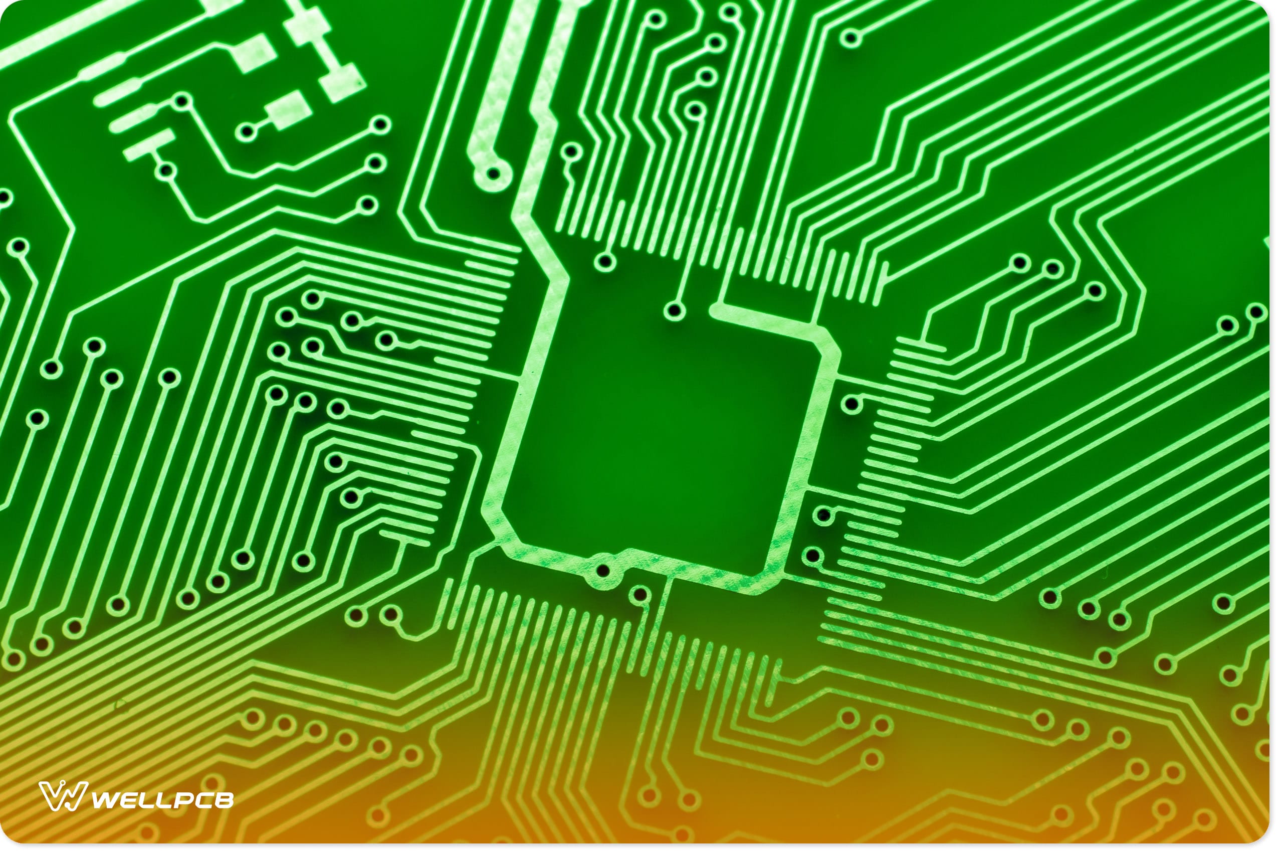
Image of printed circuit boards.
You’re looking at a 10—to 30-minute etch time. Of course, this all depends on the copper thickness, etching technique, circuit layout, and etchant. Keep in mind that the temperature and amount of the etching chemical will also play a role.
What Should You Use For PCB Etching?
The best chemical to use is cupric chloride because it precisely etches tiny features on the PCB. It also has a consistent etching rate and regenerates its efficiency.
You can also use ferric chloride — it doesn’t cost much and eats away the copper without damaging any epoxy resin. Ammonium persulfate comes into the picture, too, and etches quickly.
Conclusion
Like seriously! Etching can become frustrating if you don’t know your ways through it and with this guide, I believe you are already catching up on something. Many circuits can be etched at once; circuits can be very compact, and identical etching leading to identical circuits are some loaded benefits that etching a PCB has to offer. However, over-etching can occur as a result of an imbalance of the ratio of copper etch that is required across the board, but this problem can be rectified by adding thieving to balance it out and decrease the etchant used.
As promised earlier, wne would point out to you the perfect place to get your PCB etching materials. Wne do not only sell what we sell, but we also give a guarantee and optimum originality.
Make a move and contact us today, you can request for a quotation, and in case you have troubling questions or suggestions, please feel free to pass them across.