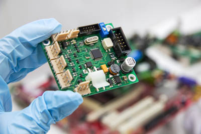
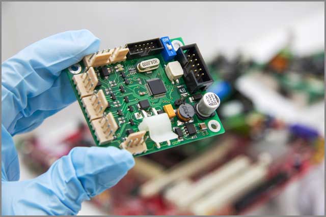
PCB fabrication is a myth for many PCB designers. They are always curious about the methods their PCB fabricators use. You would love to send your PCB design to the manufacturer for PCB fabrication and assembly. However, if you would know the PCB fabrication techniques, you could design PCBs better.
You would be able to design PCB right according to the specifications of your PCB fabricator. The development of high technology and automation technology makes correct PCB service provider. Thankfully, there are various PCB manufacturing more and more efficient. Today we would tell you about the 10 PCB fabrication techniques that you should know.
Contents
- 1 PCB Fabrication
- 2 Solder Paste Inspection (SPI) Machine
- 3 Laser Drilling
- 4 Glue Dispensing Machine
- 5 Pick-and-Place Machine
- 6 Reflow Soldering Machine
- 7 Wave Soldering Machine
- 8 Automated Optical Inspection (AOI)
- 9 In-Circuit Testing (ICT) – The Bed of Nails
- 10 Functional Validation Test (FVT)
- 11 X-ray
- 12 Conclusion
PCB Fabrication
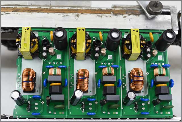
The PCB fabrication process uses four main stages to manufacture PCBs for your projects. The first stage is drilling and paste application, which uses solder paste inspection and laser drilling machines. The second stage is an automatic component placement that employs glue dispensing and pick-and-place machines.
Then, the third stage is soldering via reflow and wave soldering machines. Finally, the last stage is inspection and testing that is done using automated optical inspection (AOI), functional validation test (FVT), X-ray, and in-Circuit Testing (ICT) – the bed of nails. Now, let’s dig deeper into what these machines do.
Solder Paste Inspection (SPI) Machine
SPI machine inspects and fabricates printed circuit boards. It does so by performing a precise and quick test of the soldering paste on the printed circuit board. This ensures that the printed paste quality is high, and it is without any PCB fabrication faults. The visual methods of SPI systems monitor this paste for any errors.
It can detect flaws such as scratches, nodules, and pigments. It does so by examining the printed circuit board surface. The machine lights up the board with many light sources and has one or a camera with HD resolution. Therefore, it gets to take the image of the solder paste on the surface of the PCB. Moreover, it can also detect dimensional faults such as height, area, volume, shift, shape, overflow, and bridge. This machine for PCB fabrication mitigates the need for your manual inspection.
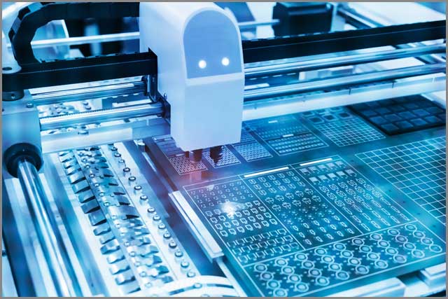
Laser Drilling
PCB fabrication process widely uses laser drilling machines. The carbon dioxide gas processes the via-holes in the interlayers of multi-layers PCB. A PCB made up of different materials such as resin for insulation of electrical connections, a copper foil to make the electrical connections, and glass fiber enhances mechanical strength. Therefore, you need to make sure that the quality of the tiny via-holes is high.
Some PCB fabricators also use the galvo scanner system with high-precision and high-speed to capture the maximum capacity of the laser drilling machine. The machine works by spatially splitting the laser beam into two identical rays through a beam splitter. Thee enhances the PCB fabrication process by processing two PCB boards together. A good PCB drilling process produces consistent, clean, and burr-free holes.
Glue Dispensing Machine
The glue dispensing machine puts glue dots on the surface of printed circuit boards before placing the board’s components. This machine for PCB fabrication will hold the ingredients to their position until the contacts and leads get soldered. You would see that this machine is particularly crucial for PCB fabrication, which uses the wave soldering process. It is because of the high force of the wave, which may displace more significant electronic components. In reflow soldering, it will help the parts falling off.
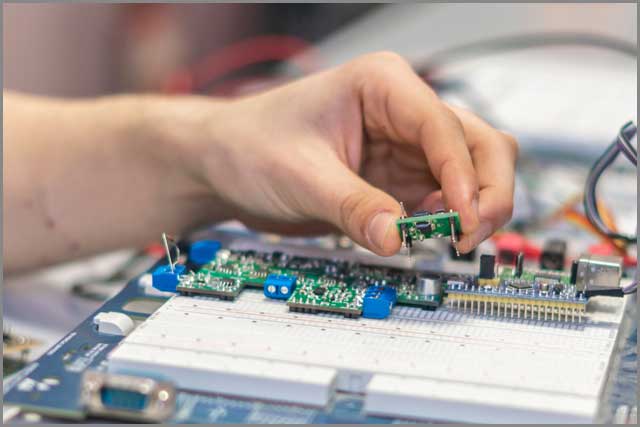
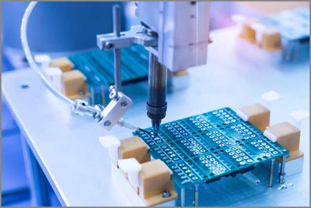
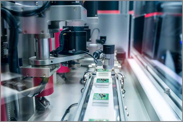
Pick-and-Place Machine
You would find this machine to be quite fascinating as compared to others for PCB fabrication. You would love to see this in working order. The pick-and-place device grasps the components and puts them onto the uncovered PCB. This machine replaces the need for the meticulous manual procedure of putting the elements in place using tweezers.
Fortunately, PCB fabricators have this automatic machine that can operate at any time and is more precise than humans. The device suctions up surface mount technology components and put them precisely at their required positions. The positions will be labeled using the Glue Dispensing machine. The machine throws the elements down at the speed of light, making it efficient enough to get a rate of 30,000 components/hr.
Reflow Soldering Machine
PCB fabrication mostly uses the reflow soldering method for accurate PCB assembly. The reflow soldering machine is a great and massive oven that deals with PCB full of electronic components. You would see that the PCB boards move via different temperature zones that the machine would be carefully monitoring. Therefore, the solder paste dissolves and strengthens to develop robust electrical connections among the components and corresponding copper pads.

Wave Soldering Machine
The wave soldering machine for PCB fabrication passes the PCB through a molten solder wave for soldering the components. At the beginning of the wave soldering process, the machine will spread on the flux layer on the PCB surface. Will clean the components’ pads and contacts, and the solder will properly stick to the board.
After that, the machine warms up the PCB to avoid thermal shock. In the end, a molten solder container builds up a solder wave through which the PCBs pass in a way that their bottom comes in contact with the solder wave. The Develops a connection among the leads of the components and their corresponding pads and holes. Nonetheless, the reflow soldering machine has taken over wave soldering because of its effectiveness for soldering SMT components.
Automated Optical Inspection (AOI)
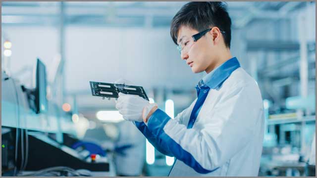
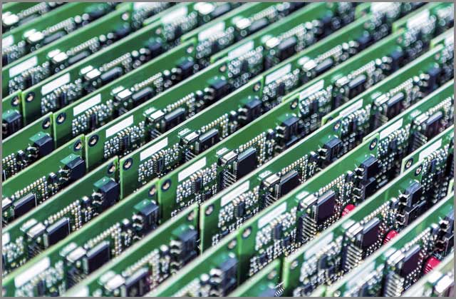
Finally, when the boards have undergone all PCB fabrication methods, you would send them for testing and inspection and testing. The automated optical inspection machine replaces the need for a hectic manual control. The naked eyes cannot accurately inspect multiple PCB boards and when they produce on a large scale.
In PCB fabrication, AOI machines identify glitches in the PCB early on in the fabrication process. It utilizes HD cameras to take pictures of the board’s surface and then do its analysis. The machine compares the images with reference images to identify the faults. It will save wastage of PCB material and the cost of re-manufacturing. Moreover, this fixes the individual boards early, and the methods are accordingly modified.
In-Circuit Testing (ICT) – The Bed of Nails
The in-circuit testing phase uses a bed of nail fitting to inspect the working of complex PCB boards quickly. The testbed has an arrangement of pogo pins, and each one of them connects with nodes in the PCB circuit. The final PCB is put on these pogo pins and pushed downwards to make circuit board shopping, various things might get you confused. Whether you are going for a single-sided PCB, a double-sided PCB, or any other type of PCB, You can contact with test points. The pogo pins fitting quickly send test signals through the PCB via these test points. Therefore, it identifies any shorts or breaks in the circuit.
Functional Validation Test (FVT)
As the name implies, this test uses software to check if the PCB will work according to its function. It should be able to perform precisely what you want it to in your required field of application. The functional validation test interfaces the PCB through the test point or its connector for simulating the working environment.
The details of functional validation tests vary from product to product, as every PCB is unique. Commonly, the PCB fabricators personalize the hot mock-ups set up to simulate the final working environment. However, it does not matter how we customize the FVTs as they all have the same software, hardware, and components.
X-ray
Many modern PCB designs include lead-less package types such as QFN and BGA assembly. These components make connections with PCB under their bodies. Hence, traditional inspection methods are not efficient enough to inspect the internal structure of the PCB. The automated X-ray inspection method of PCB fabrication tests the hidden attributes of PCBs using X-rays.
To ensure the quality of the PCB fabrication process, an X-ray penetrates the PCB package’s into the PCB package’s internal layers. It then examines the quality of soldering connections. The advantage of X-ray is that the PCB materials absorb it according to their thickness, atomic number, and density.
Conclusion
So, these were the 10 PCB fabrication and assembly techniques that you should know. Wne are hopeful that now you would see the big picture of what we are doing at the back-end. Wne fabricate high-quality PCBs using all of these machines and in no time. Feel free to development of flex PCB. Our dedication is to manufacture high-quality flex PCB. If you are looking for the right flex PCB manufacturer, contact us if you have any questions or want to ask for a quotation.


