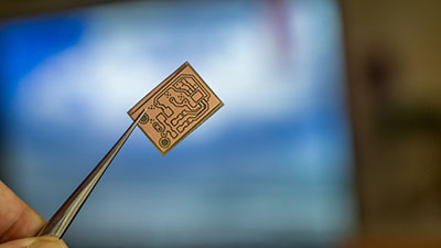
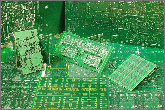
The printed circuit board or PCB, in short, are boards that connect electronic components. Non-conductive fiberglass is the crucial material known as substrate. A coating of a thin layer of copper is on either one side or both sides of it. The etching of lines, pads, or vias is on the copper plate and excess copper removed. If you want to see what kind of PCB?
Open your discarded or destroyed electronic devices, whether be it PC or laptops. You’ll see a thin green board with etchings on it, which I am sure you have already seen before. They look quite beautiful.
Many of you don’t know much about multilayer PCB, but almost every primary electronic device has it; yes, they do. So here it is, everything you need to know about multilayer PCB.
Contents
1. What is a Multilayer PCB?
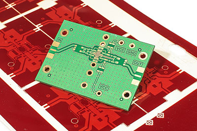
PCBs, come with a single layer, double layer as well as a multilayer. Single-layer PCBs have a copper coating and etching on only one side of the board. Double-layered PCBs has it on both sides. Another thing every layer has some print on it irrespective of the multilayer PCB.
What makes a multilayer PCB different from a single or double-layer? It is its sandwiching of fiberglass between layers of copper. The number of layers can go from 4 to 28, with a thickness of 0.4 – 5 mm in sophisticated electronic devices.
1.1 Where do you Use Multilayer PCB?
From mobiles to laptops to heart monitors, all use multilayered PCBs. Why do you ask? It’s because of the increase in functionality from a single or double-layered. Think of it like this when you need complex circuit connections.
One can do this with either multiple single-layered PCBs or a single multilayered PCB. This not only increases the functionality but also decreases the weight — another thing it takes up a lot less space than single or double-layered PCBs. The results are smartphones, TVs, laptops getting extra thin.
1.2 The Top Benefits of Multilayer PCB
- Higher functionality and capability
- Takes up less space
- Less weight compared to single or double layer
- Faster speed
- A higher density of components
- Both rigid and flexible manufacturing is possible
2. The Top Questions for Multilayer PCB
Now you know what a multilayered PCB is. Let us dive a bit deeper and talk about the technical things associated with it. Do not worry, it is not dull, and you do not fall asleep.
Here are some things to keep in mind while messing around with PCB.
2.1 What Kind of Working Frequency Do You Need?
Imagine clicking on an application in your device and waiting for it to open. You keep on waiting. Sometimes it is super slow.
I am sure that it does not put you in a good mood. Well, that is because of the clock speed or frequency of your processor (also a PCB). Single layered or double layered PCB has a working frequency of around 500 MHz – 1 GHz.
Multilayered PCB has a working frequency of 500MHz – 2 pretty high GHz. If you feel like it is not much, then my friend, you are wrong, it is enough to get an application to open a minute faster. The current century is all about speed and streaming, faster devices, faster life. And everyone wants to be a bit faster, whether it is by a few seconds or a minute.
2.2 Density of Multilayered PCB
Did you take a look at PCB boards carefully? You will see structures that look like cities with different roads. It is pretty cool, to be honest. The components have a higher density than a circuit board of a typical LED.
With devices getting thinner, there are more components in a single circuit board. And the way to do that was yeah you guessed it right, multilayered PCBs. But designing a PCB with a higher density of components is by no means a walk in the park. It takes severe head-banging and various considerations. You need to know the number of ground planes, power planes, and vias.
Will you use buried or blind holes?
Blind or Buried vias
Vias are holes on circuit boards drilled to connect components in the inner or outer layer. Blind vias connect the outer layer of the circuit board to the inner layer. Buried vias connect internal layers, which appear as a blank spot if you look closely.
Aspect ratio
It is the ratio of the thickness of the plate to the diameter of the through-hole of the hole. Generally, the aspect ratio is 6:1 by most manufacturers. A smaller aspect ratio allows for greater strength of the PCB. The higher aspect ratio allows for more copper plating and frequency. So, you need the right balance while designing your PCB.
Signal Integrity
The signal can go from one point to another without loss or distortion. If your signal integrity is not right, then your PCB is not working well(if you are Sherlock, you will know it). That is why you need a proper arrangement of ground planes, power planes, PCB material, and vias in mind.

3. Rules for Designing Multilayer PCB
Now, we have flashed past the technical things (phew); let talk a bit about designing it. It can be fun and exciting. If you plan on making a PCB, here is what you can do.
Step 1- Make a schematic diagram, which is a blueprint for all your components on your PCB. You can do it with the help of a software or by hand, but I recommend software.
Step 2- Draw the board layout. You can do it with the help of software such as KiCad and Circutimaker. Just Google it, and you will find a lot of software.
Step 3- The last step is etching on the circuit board. You can get it done by someone else as some businesses offer this facility. Or you can do it yourself with the help of a solder gun and other things.
You also need to make sure that your schematic design is correct and not just beautiful. Designing a PCB is pretty fun. However, don’t go overboard. And try to make a PCB for a graphic card when you are starting.
I’ll recommend you to start with LEDs. They look pretty cool. Plus, it is a pretty good hobby as well as a pretty good work to do in your spare time.
4. Different Types of Multilayer PCB
So, what are the top types of multilayer PCBs? Here is a look.
Single-layer PCBs – It is one in which copper layer [thin] coating is on only one side of the board. On the other hand are connections of electrical components connected electrically.
Double layer PCBs – In this type of PCB, a thin layer of copper coating is on either side of the board. Drilled holes connect circuits of both parties.
Multi-layered PCBs – It is a series of 3 or more double-layered PCBs. Insulation is between each PCB. They are in place through powerful glue.
Rigid PCBs – These PCBs use rigid substrate, which does not twist. It comes in a single layer, double layer as well as multi-layer PCB.
Flexible PCBs – These PCBs use flexible substrate material. It also comes in a single layer, double layer as well as multi-layer PCB.
Note: You can use aluminum as conductive material other than copper.
5. Multilayer PCB– Application Areas for Multilayer
I know you already have a pretty good idea about the fields of PCB use. So I’ll tell you a little about various places you can see it in.
• Electronic devices, such as computers and smartphones. Almost all electronic devices use some form of PCB. It can be in pure form or complex, sophisticated form.
• Medical devices such as heart rate monitors and CT scanners.
• Home appliances such as microwaves, refrigerators, and coffee makers.
• Lighting equipment such as LEDs and neon signs.
• Industrial equipment, such as drills. Or, automotive equipment such as navigation devices and control systems in cockpits.
These little thin boards have infiltrated every walk of life. They are everywhere around us.

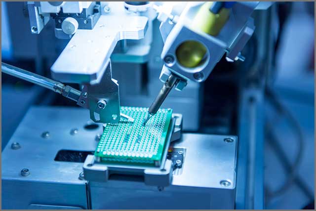
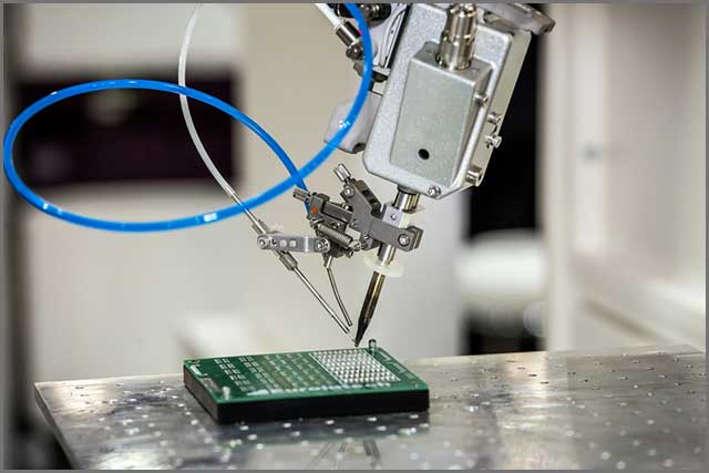
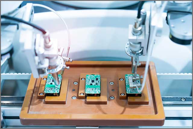
6. Manufacturer of Multilayer PCB
Manufacturing multilayer PCB’s can be quite tricky, as you will know from this video. The process is very intensive and demands accuracy.
• There is a sandwiching of multiple layers of copper foil, prepreg, and cores. This sandwiching process requires very high pressure [50psi] and temperature [350F].
• During sandwiching, even stress on layers is necessary. Failure in doing so will result in uneven pressure. Or, cause uneven thickness at different positions.
• All layers have to be in alignment.
If you are looking for customizable multilayer PCB’s and don’t know where to start, look no more. We offer customizable multilayer PCB’s for your needs.
Summary
Multilayered PCBs saw an increase in its use during the 80s. Today, it has become an irreversible part of our electronic devices, which are here to stay.
The global PCB market will reach around 90 USB$ by 2024, with a compound Annual Growth Rate of 4.3% for 2019 – 2024. Multilayered PCBs are way more useful compared to single or double-layered PCBs.
But at the same time, they are costly, need a lot of investment in technology, time, and optimization. So, if you plan on designing a PCB, whether it is for fun, for some project, or your interest, act on it. Talk to us about your multilayer PCB needs. We are a PCB manufacturer you can trust.