It was more than seven decades ago when the first PCB was designed. Ever since then, this component has become an integral part of many electronic devices. Have you ever wondered what the future of printed circuit boards has in store? That is what we are focusing on in this article. Keep reading to learn more about the future of PCB technologies and how that will affect other industries.
Contents
- 1 How 3D Printing Can Affect the Future of PCB Technologies
- 2 PCB Technologies–The Importance of Autoplacers
- 3 Why High Speed Is Essential for the Future of PCB Technologies
- 4 PCB Technologies–What Are the Types of Signals Used in PCBs?
- 5 PCB Board Cameras
- 6 PCB Technologies: Flexible and Biodegradable Printed Circuit Boards
- 7 Conclusion
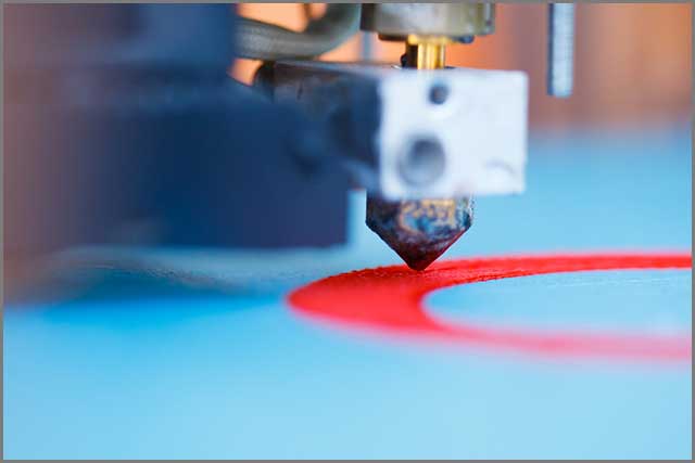
How 3D Printing Can Affect the Future of PCB Technologies
Today, you can see 3D printed products used everywhere. 3D printing is one of the innovations that truly revolutionized the market across numerous industries. The sectors that benefitted range from automotive and firearm to art and architecture.
It was only expected that 3D printing would change the PCB industry, too. It seems that this technology already changed how electronic systems work from the ground up, and this is only the beginning.
The way 3D technology works in the PCB industry is that individual printers follow the design and print the circuits one layer at a time. Once the printing part is over, experts use surface-mount technology to complete the manufacturing process.
Advantages of 3D Printed Electronics
Comparing the new 3D approach to the previous 2D PCB technologies will discover that the former has multiple advantages. These include:
♦ Additional design options – the fact you can print the circuits on top of the desired shape gives you a lot of freedom when choosing the design. It is an excellent way to scale all electronic, mechanical, and optic functions to any desired size and shape.
♦ Boosted efficiency – 3D printed electronics will use less material than 2D manufacturing. The additive process ensures that there is no waste of material left after the procedure. Apart from the efficient use of materials, using the 3D approach minimizes room for error. Digital production ensures the highest level of accuracy. Although there is still a small chance for failure, it is far less than in the 2D manufacturing process.
♦ Eco-friendly – 3D printed electronics allow you to use virtually any material for your PCB needs. That means you can go with materials that cost low and those that are eco-friendly and recyclable.
All these benefits mean that 3D manufacturing is a step forward compared to the 2D process. Not only is mass production more manageable and affordable, but you can also show corporate responsibility by using eco-friendly materials. Although it is still not widely used, the chances are that more companies and industries will adopt the 3D approach over time.

PCB Technologies–The Importance of Autoplacers
The majority of PCBs nowadays use autoroutes. These parts ease the automation process, but they are not easy to set up correctly. Moreover, their design might require plenty of time and effort. Although you will save time during the PCB manufacturing process, you will lose it while constructing the auto-router.
That is why the industry is looking for an alternative, and it may come in the form of auto places. These automate and simplify the process by integrating electrical and mechanical CAD systems. The problem is that auto places still haven’t reached the reliability level used in mass production.
What Is the Difference Between Autoplacers and Autoroutes?
♦ Autoroutes – available properties include choosing the desired layer number and directions, the distance between the connections, and spacing between tracks.
♦ Autoplacers – mechanical considerations drive the constraints that are in charge of component placement. It is a new technology that still needs plenty of improvement before being used in mass manufacturing. If that becomes possible, it could accelerate the process significantly.
Why High Speed Is Essential for the Future of PCB Technologies
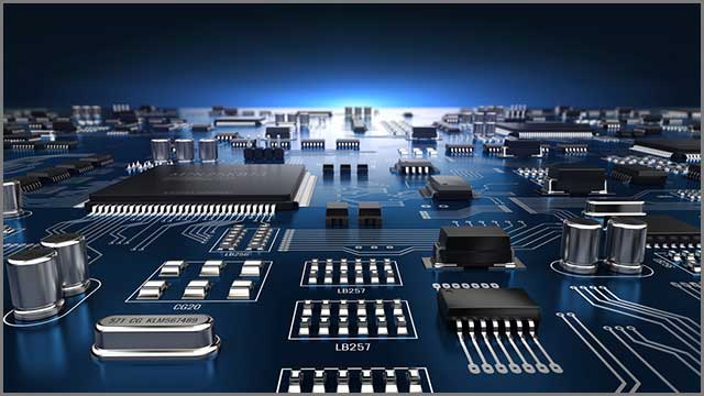
Caption: Printed circuit board – 3D illustration
We live in a fast world, so it doesn’t seem strange that speed is essential in every asset of our lives. As we see full versions of electronic products, we also notice the desire that they perform even faster.
That is why extra speed is one of the primary considerations of PCB designers. It is not easy to define what constitutes a high-speed PCB. According to the majority, it seems to be a printed circuit board where the circuit layout affects signal integrity.

PCB Technologies–What Are the Types of Signals Used in PCBs?
♦ Analog – the intelligence comes in a signal shape. If there are integrity issues, you will notice the altered forms of the signal.
♦ Digital – the intelligence comes in digital pulses. In case you notice any integrity problems, they can be shown as canceled or delayed signals.
The signal’s integrity may be disrupted by various factors, such as track length, distance from other signs, PCB’s dielectric, etc. That is why it is essential to avoid these potential issues.
Designers are often creative, but that doesn’t change that new PCB technologies could further improve the results. It shouldn’t be a surprise if we see innovations in this field in the future.

PCB Board Cameras
Printed circuit boards have already progressed enough that cameras can be one of their components. It would help if you directly mounted the camera onto the PCB, and the unit will take photos or record videos.
PCB Technologies–What Are the Benefits of PCB Board Cameras?
As you might assume, these cameras are tiny, making them suitable for almost any board and electronic device.
Although they started modes, PCB cameras made tremendous progress, and they are still being perfected to provide even better pictures and videos.
Potential Applications of Board Cameras
The compact size means versatility, so there is a wide range of potential applications for PCB board cameras. These include:
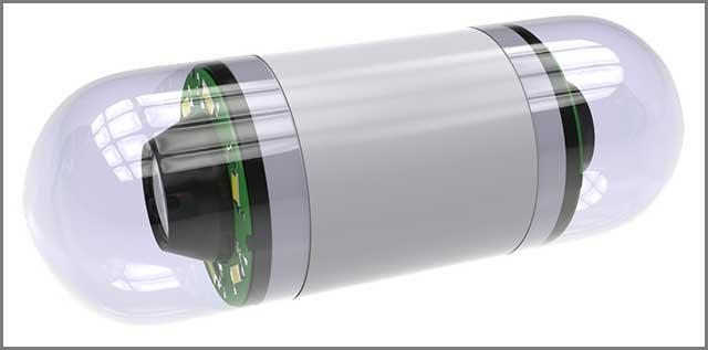
♦ Medicine – these devices can be beneficial in both invasive and non-invasive procedures. Cameras usually come in the form of a pill that patients swallow. These capsules can be used in many procedures, such as capsule endoscopyrel.
♦ Surveillance technology – the compact size makes the cameras great for surveillance purposes. You can see home and business owners placing these cameras around their houses and offices.
♦ Consumer Electronics – laptops, tablets, smartphones, and other portable devices often come with a camera. The noticeable trend is to keep making cameras deliver better results while reducing their size.
Some of the camera features that could be improved in the future are low-light conditions, durability, and image quality.
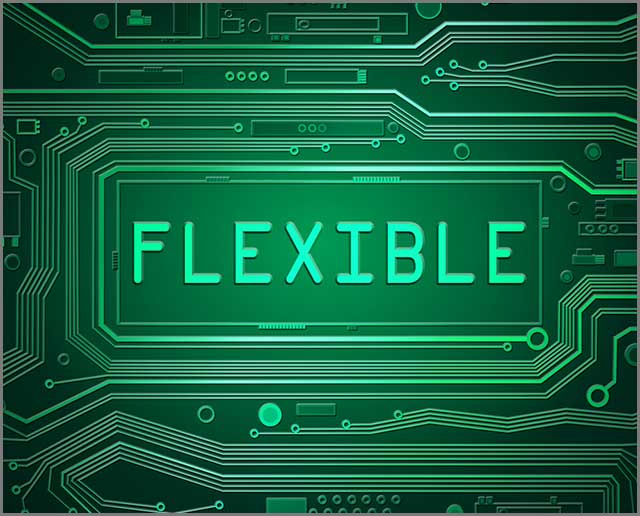
PCB Technologies: Flexible and Biodegradable Printed Circuit Boards
WellPCB offers DC motor controllers in both domestic and international markets. We have Flexible printed circuit boards that are becoming more popular, and their sales numbers increase every day. Many industries adopted strictly flexible and flex-rigid PCBs due to their increased flexibility.
It is the bendiness that is the main benefit of these boards. If you have a compact space and use a bendy board, this can be a great choice. Other benefits include the fact that they are thin, lightweight, and suitable for mass production. Thanks to that, you can fit a flex PCB almost anywhere.
PCB Technologies–What Industries Use Flexible PCBs?
Here are only some examples of industries that adopted flex boards:
- Medical instruments – apart from compact sizes, flexibility means a lot for medical devices. Flex PCBs are reliable enough to be used in many medical instruments, such as sensors, monitors, implants, and surgical tools.
- Flexible displays – you probably heard of smartphones with flexible screens. It is the most common example of using flex printed circuit boards. These PCBs are better at absorbing shock, but their manufacturing is still quite expensive.
- Wearable technology – smartwatches and other “smart” accessories often use flex boards. They perform better in terms of shock resistance, which makes them a great choice.
- LED lighting – flex PCBs play a key role in LED strip lighting as they enable the consumer to adjust the product to their needs.
Many companies out there can deliver flexible PCBs, but few are as reliable as WellPCB. The experienced engineers can respond to all client’s requests and manufacture rigid, flexible, and flex-rigid boards. The automatic quoting system on the website allows you to customize and place your order efficiently.
Biodegradable PCBs
Caring for the environment is essential for the future of the planet and shows corporate responsibility. Companies look like they are racing to make the best eco-friendly solution when designing smartphones, tablets, and appliances.
Electronic waste is a big problem, and printed circuit boards are one of the causes. The choice of materials to design PCBs is not always the best as it is not degradable and often ends up as a pollutant in landfills. In short, any outdated PCB might harm the environment.
The industry is looking for eco-friendly alternatives that could be used instead of current materials. Some materials are under review, which means we may see them approved for mass manufacturing. Although we may not see 100% biodegradable PCBs any time soon, the industry is leaning towards using at least some more environmentally friendly components.
Conclusion
We see innovations in technology every year, and the PCB industry is no exception. While printed circuit boards have already been elevated to a high level, there is still room for progress.
The challenges include increasing the speed capabilities and identifying eco-friendly materials and processes that could simplify the manufacturing process. It will be exciting to see the development of PCB technologies in the future as we are certain that it has great things in store for all of us.