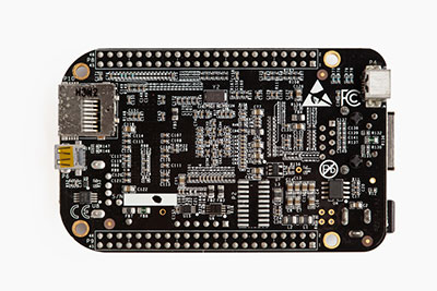
So, are you all set to design your first PCB prototype? We are sure this must be a eureka moment for you. We appreciate your desire to innovate and try something out of the box. However, if you are confused about further designing your PCB prototype at a low-cost PCB, this article is for you!
Here, we will provide you with a deep insight into PCB prototyping. No matter if you are a newbie or an expert engineer, we are sure these steps will benefit you immensely.
Let’s get started.
Contents
- 1 Why Printed Circuit Board Cost is an Important Criterion
- 2 Dimensions
- 3 Number of Layers
- 4 Material
- 5 Plating Finish
- 6 Board Thickness
- 7 Impedance Control
- 8 Hole Sizes
- 9 Solder Mask
- 10 Stick to Industry Standard Sizes
- 11 Core Components Selection
- 12 Circuit Design
- 13 Low-cost PCB–Bill of Materials
- 14 Low-cost PCB–Experiment and Repeat
- 15 Conclusion
Why Printed Circuit Board Cost is an Important Criterion
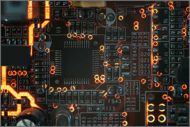
The cost of your printed circuit board is an important criterion. The more will cost, the expensive your final product will be. As a matter of fact, circuit boards can cost anywhere from 50 cents to $300 and could go much higher depending on the complexity, the number of layers, and what you plant to mount on them.
Dimensions
If you want to keep the cost of your PCB prototype as minimum as possible, it is essential to keep its size in check. Quite predictably, the price of a PCB will go up with an increase in its surface area.
Similarly, PCB board designs with irregular shapes will cost more when compared to conventional forms. Because of the large amount of waste generated during fabrication.
Number of Layers
As it goes, the higher is the number of layers in a PCB; the more will be its complexity. And the more complex a PCB design is, the costlier the entire process will be.
Thus, it is highly recommended to keep the number of layers as limited as possible. A better approach here will be to have additional PCB copper layers that are stacked on top of one another in the form of highways. They will provide a new plane for the routing of electrons and serve the purpose well.
Material
If you want to keep your PCB prototyping cost as minimal as possible, it is essential to focus on its material type. The standard PCB is made of copper. Other accessible PCB materials used include glass epoxy, also known as FR-4. Here, FR stands for flame retardant, and the number in front of it stands for its flammability.
FR-4 is the default choice of most PCB manufacturers. However, in the design of the dielectric constant and thickness of the material is essential for high-speed board parameters, care must be taken.
Plating Finish
With a pad plating process, the exposed copper surface of the PCB cover with another metal material. This is to improve the solderability of the pad during assembly. The two standard techniques include HASL and ENIG. If you want low-cost PCB prototyping, you must stick to HASL as ENIG is quite costly.
Board Thickness
The thickness of the PCB also plays an essential role in determining the PCB fabrication cost. A depth of 1.6mm seems to be the industry standard, but it might go up depending on the number of copper layers.
The thicker board determines your production costs. In modern technology, thick boards are costly, but their functions are not very comprehensive. Instead, it is a thinner board that can use in mobile phones and electronic products. When designing a PCB, you have to decide the thickness of the PCB you need and then develop it later. Avoid some problems.
Impedance Control
If you plan to integrate Bluetooth, Wi-Fi, and the related technologies on your PCB, it is essential to define the impedance accordingly.
The PCB impedance depends on several factors, including trace width, pre-preg material, and solder mask. It is essential to have proper impedance control to optimize wireless antenna performance.
However, since most manufacturers won’t provide you with controlled impedances, this will serve as an additional expense.

Hole Sizes
Determining the right hole size on your PCB is critical. Holes help in creating vertical electrical connections between copper layers. Although small pads can help you save space (thus, saving cost), it could make the process difficult for the manufacturer.
Further, too small holes would also mean tighter tolerance and could create more waste, thus costing you more.
Here, the best way is to keep the things balanced and go for holes in the range of 0.2 – 0.3 mm.
Solder Mask
A layer of lacquer-like polymer is applied to the copper traces of a PCB. It prevents the formation of solder bridges and rules out any possibility of short circuits.
Unquestionably, solder masks are essential. If you need to design a low-cost PCB, we can only choose the type of solder mask and the printing method.
There are many types of PCB solder resist, such as:
1. Epoxy liquid
2. Liquid photosensitive imaging
3. Photosensitive imaging of dry film
4. Top and bottom masks
You can choose according to the specific design of the PCB function. If you need particular help, you can contact us, and we will be happy to provide services to choose the most suitable for you.
Stick to Industry Standard Sizes
If keeping the costs as minimal as possible is one of your main motives behind PCB prototyping, It recommended avoiding reinventing the wheel. Stick to the industry-standard sizes as much as possible.
Because most manufacturers follow these standard industry sizes and have their equipment tailored to these requirements if you require anything out of the box, the manufacturer will have to make extra efforts. in turn, it will impact the custom PCB cost adversely.
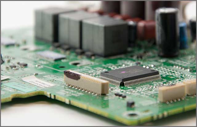
Core Components Selection
For efficient prototyping, you must have a clear idea of what all electronic components like sensors, microchips, displays, sensors, and connectors do you wish to deploy. The target price of the final product will also play an important role.
The best way here is to create a related block diagram to ensure natural coherence as detailed as possible.
You can use PCB design software for preliminary design and have an initial document for the PCB layout. In this way, some PCBA calculators can be used to calculate the cost promptly.
Circuit Design
Once you have a basic idea of what is needed and other expectations, it is time to create a schematic diagram of the design. You can take the help of design applications to make this task easier. This diagram will also provide you with a more in-depth insight into how different components will connect among themselves.
Once you have designed a preliminary schematic, contact us at WELLPCB, and we can give you everything you want to know about this board.

Low-cost PCB–Bill of Materials
Once the manufacturing of PCBs, there are high chances of layout failures, which can go a long way into negatively affecting the final product’s functionality. There are several PCB layout is complete, it is now the right time to generate the materials bill. It can be created automatically through the schematic design software. The proposal consists of the part number, quantity, and other specifications.
You can then analyze the bill and see what costs the most for future analysis and improvement.
Low-cost PCB–Experiment and Repeat
Get the PCB back from the manufacturer and assess it correctly. Likely, your PCB may not meet your requirements. Don’t be surprised. Things often do not go as expected.
The time that you must weigh your options thoroughly and work on your PCB to debug it.
This part may cost you a lot of time, but I think it is worth it because you can find problems and solve them. This is related to the function is made PCB.
Conclusion
how you can design a low-cost PCB prototype. The key here is to stick to the industry’s standards and follow the best practices to keep the printed circuit board costs minimum.
Additionally, your PCB manufacturer also plays an important role. Choose to go for the one who welcomes prototyping orders whole-heartedly and offers reasonable prices. They must also offer discounts and be equipped with the right tools to simplify manufacturing.
What are your views on this? How do you ensure easy prototyping at budget prices? Do let us know in the comments below.
