There are many things that PCB CAM (Computer-Aided Manufacturing) software can do for you. The most important role is its ability to analyze production files and aid in PCB production. No matter which project you’re working on, PCB design breathes life into your electronic circuit. Let’s think about technological advancements.
We had moved past those days when PCBs laid out with masking tape or programmed surface mounts machines. Layout software combines component placement and routing to the PCB design process to define electrical connectivity on a manufactured circuit board. Sure, the traditional approach is still usable. But why would you, when current tools make it much easier and more precise? This article guides you to know everything related to how CAM Process helps in Prototyping.

(CAM sign – circuit board style)
Contents
- 1 1. What is PCB Computer-Aided Manufacturing (CAM)
- 2 2. PCB CAM–CAM handles the content
- 3 3. CAM running components
- 4 4. PCB CAM–Difference between CAM and CAD
- 5 5. Schematic diagram of PCB CAM data output
- 6 6. Things that CAM can help you/why should we use CAM
- 7 7. Consequences of skipping a CAM test
- 8 Summary
1. What is PCB Computer-Aided Manufacturing (CAM)
To begin with, Computer-Aided Manufacturing (CAM) is the automation of computer-controlled machinery and software in manufacturing. Before the correct PCB service provider. Thankfully, there are various PCB manufacturing process, manufacturers receive designers’ files in various formats. These files mainly contain information on; wire wrapping, component insertion, routing, and many other design details of the required PCB.
CAM software analyses the files and identifies the format. After this, you can then recognize the file format, drilling data, and artwork layers. So, it’s checked and accustomed to guaranteeing manufacturers build up the board according to its original design on receiving PCB artwork. A reason that sees it is one of the system positives. On analysis, when a file is missing, the project stops, requiring an extensive DRC. Design Rule Checking verifies whether a design meets the standards imposed for manufacturing.
PCBs have evolved completely, from wood pieces to sophisticated green boards. They were earlier associated with only computers, and now with microelectronic, everything is drowning in PCBs. Apart from the PCBs are everywhere, in industry machinery like motor -controllers or industry load testers. Even lighting in some places uses PCBs.
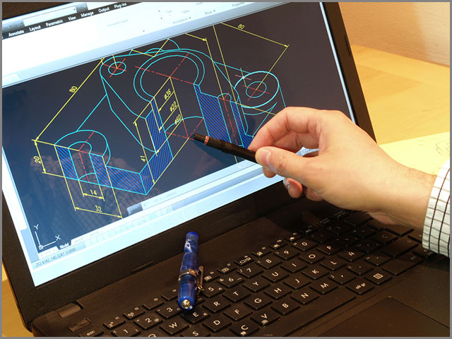
(a designer working on a CAD design)
2. PCB CAM–CAM handles the content
Our world is full of material things, whether they are products, places, or parts, and CAM makes it possible. We give the power of flight to airplanes or the thunder of horsepower to automobiles. Whenever you want something made and not roughly designed, CAM is the answer.
CAM prepares files for production. For that reason, you can think of CAM as a “slicer software.” It relates drawings and data into specific instructions for driving an automated tool.
It uses G-code, a programming language generated from a drawing, to communicate with the control machine. The code instructs the device on what to do. For example, it will lead the motors to move, how fast to do it, and the programmed path they should follow.
The software also checks for errors. For instance, it can assess if the model has any geometrical errors that can alter the manufacturing process. It also generates a toolpath, a set of coordinates that the machine needs to follow during the machining process. A good example is setting a cutting sequence. Before any operations start, pierce heights, voltage, and cutting speed have to be adjusted parameters. Different programs can set various parameters when accurately defined. These parameters depict the machine operators’ work making it much more comfortable.
3. CAM running components
Software
CAM software performs several tasks once the design files come in:
- It translates electronic data into images for checking, viewing, measuring, and editing data.
- Performs the Design Rule Checks (DRC) comparing the IPC Netlist with imported data
- It recognizes the drilling data, artwork layers, IPC Netlist, e.t.c format.
- It also verifies the layer order sequence.
Post Processing
Postprocessor is a software sub-program that alters non-graphical and visual CAM system into a correct numeric control. It’s also independent of hardware adapting toolpath into machine-readable motions or language. So, the postprocessor is a crucial driver specific to a mechanism or machine. Some machines have different movements between operations, or they start at distinct locations. The CAM program analyses the CAD model computes the correct tooling and toolpath, which will mill the intended features.
Machinery
CAM machinery is the final stage transforming the raw material into a finished product. The machine can either move forward or backward, creating a prescribed motion in the contacting element called a follower. The prescribed movements and the follower’s profile determine the shape of the CAM contact surface, which may be flat or circular.
There are various forms of CAM machinery. They include;
- Rotating plate with the correct profile
- Plate fitted with a groove cut on its face, which includes a roller on the follower.
- Cylindrical member consisting of a track cut around its surface
- Cylinder with the correct profile cut in the end
CAM, as a rotating machine element, gives oscillating motion to a follower. The CAM and follower have a high point of contact, which then makes a higher pair. There’s also an external force provided by a spring that upholds the connection between them.
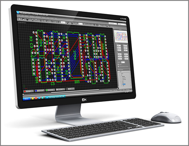
(An example of PCB software at use)
4. PCB CAM–Difference between CAM and CAD
Introduction to CAD
Computer-Aided-Design (CAD) software enables designers to build models in an imaginary space. CAD creates two and three-dimensional physical models, replacing the manual pencil on paper approach design and engineering.
Most readers are familiar with the 2D CAD model. 2D drawings are flat and provide comprehensive dimensions, layouts, and needed information. These types of pictures may be necessary for various industries, including automotive, architecture. If you have ever built a house, you can still remember the small fortune you had to fork over for your floor plans. The architecture who designed them without a doubt used CAD to create them.
3D and 3D CAD models have similar uses, then where is the distinction? A 3D CAD model provides greater depth to the components and assemblies of a physical object. It shows how things fit together and their operations, not only how big or their overall shape.
Technological advancements have automated the manufacturing process with software and robot involvement. CAD being the core pillar of these processes, has changed the rules of engagement. Industries have evolved following the best standards, and CAD has transformed PCB innovation.
CAD Netlist
Look at your schematics, think of what would you do if you had to transfer the schematic into a PCB layout tool? What is the efficient way to do it? After that, you may try stripping out the visuals and share the connections between components. If the net is the connection between two computers, a netlist is a list of electrical elements that describe a circuit. It is important to note that it varies in formats and the information they convey.
Understanding how to read the netlist list will help in troubleshooting errors. A schematic and its netlist go hand in hand. You can generate netlists from schematics or (flat or hierarchical)schematics from the netlist. About information in a PCB schematic, a netlist consists of multiple entries of data. The CAD Netlist usually received in several formats, including
IPC-D-356
IPC-D-356 is an electrical test format traditionally designed for supplying Gerber files with Netlist descriptions. It now defines a standard Netlist format on which you can represent bare board test information. It means that it is capable of storing specified coordinated instructions and designating PINs. Done right, IPC-D-356 may contain all information a test system might need in performing a bare board check in a single consistent file.
ODB++
ODB an acronym for Open Database, a proprietary CAD-to-CAM data exchange format that is useful in manufacturing and designing electronic devices. Its development accommodates the PCB board designs to transfer information among manufacturing, design, and design tools from different vendors. Various companies manufacture CAM and CAD software. So, they agree on a level data transfer system for CAD-CAM, and ODB++ facilitates these transfers.
G-Code
The G-Code “Geometric code” is for CNC machines (Numerical Control). The G Code handles the communication of gears and motors in the machinery. They instruct it on how to operate and complete a task. These commands drive the machine following a specific tool path.
At first glance on a G-code file, it looks complicated, but in reality, it’s not that hard to understand:
G01: Linear Interpolation
In the first place, this code command instructs the machinery to move in a straight line at a set rate and speed. By specifying the positions and speed, the machine controller computes the valid points. Other individual codes range from G00-G003 and G17-G21.
F20
In G code, F refers to words and addresses. F represents the letter, and the address is the following number. An example is when a machine using the imperial units “F20”. It communicates to the device to move 20 inches per minute.
S500
In G code, S refers to spindle speed (RPM). The word represents spindle, followed by RPM’s. An example is when you type in “S500,” S tells the spindle to start spinning, and it will do so at 500 RPMs.
T01
Manual insertion of a tool into the spindle tape is possible; you only need to know how to do it. Tool changing is a two-step process on a mill; first, you select the T-word tool, followed by a number, e.g., T01. Then follows the tool change, e.g., M06. You can also put them or write them together.
Differences between CAM and CAD
To begin with, let’s explore some of the similarities that both CAM and CAD share.
- Both CAM and CAD are essential tools in manufacturing and design. Before the computer system’s short evolution, drafters used to perform critical design roles. Computers then changed the scenario; they were both affordable and flexible.
These changes allowed manufacturers to draft schematics freely. CAD and CAM are irreplaceable in the field of design and manufacture.
- CAM is the use of computer-controlled machinery and software to automate manufacturing. CAM assists engineers and machinists in creating or prototyping PCB. CAD has many functions independent of CAM, but CAM over-all is dependent on CAD. Without CAD, CAM may not exist. CAM software supports.
- Both CAM and CAD are critical parts of a necessary process in Computer-Aided Engineering (CAE). CAM and CAD render items in 2D and 3D; they help in fast processing and production of every designed concept.
- The notable similarity between these two systems lies in the end-user. Both programs depend on trained operators for instructions to fit the correct specs.
Differences
So, what are the significant differences between CAM and CAD?
- CAM system demands both control and coordination of the physical process, labor, equipment, and material. In contrast, CAD involves product design concepts and analysis.
- CAD requires computer use for transforming product design concepts into detailed engineering designs. The process involves the creation of geometrical models that have undergone manipulation and in-depth analysis. On the other hand, CAM requires computers to assist engineers, managers, and production workers, whereby they automate production jobs by controlling machines and systems.
5. Schematic diagram of PCB CAM data output
CAM supports production and prototyping. The primary aim is numerically controlled drilling and inserting components. A computer-based controller, in the numerical controller, translates a list of codes into instructions. The machine tools immediately understand the translated instructions.
Preparations before PCB CAM process
The most important information obtained by the PCB manufacturer is the Gerber file and PCB information. Gerber format is an open binary 2D vector image file format. PCB software industry uses it as a standard file format to describe PCB images for copper layers, solder masks, legends, etc.
In the operation process, engineers optimize Gerber files placing in mind available factory equipment and processing power. They then prepare the manufacturing manual/instructions to suit the firm’s capability. The Gerber review, CAM manufacture, usually takes a day.
Currently, rigid boards command a significant share in the PCB world. You should also note that IPC6012 is the basis for manufacturers to carry out PCB design and processing. So, designers need to understand several processes required by the PCB processing plants for PCB design.
For desired rigid PCB outcome for manufacturers: line width 3mil, minimum. Mechanical size drill 8mil, minimum laser drill 4mil. BGA minimum PTH hole to hole distance 8mil. The limit in design leads to a decline in the product qualification rate and cost increase. It’s recommendable that you examine your ideal PCB manufacturer’s capabilities in the design world.
The designed minimum of the line spacing, BGA, hole, etc. on the circuits diagram affects yield. In turn, it influences the processing cost. The designs must be as large as possible under a reasonable layout of the circuit, a single board’s panelized, suiting the production line.
Sometimes making smaller PCBs doesn’t influence the cost since the copper cutting. You could fix the Clad laminate to reduce costs. It’s recommendable that you communicate with PCB manufacturers to understand the design boards. Also, be willing to accept guidance to achieve the utmost use of the PCB board to reduce the cost.
PCB CAM–Design choice for the copper layer
PCB technologies have evolved, and therefore consumers demand faster and more robust products. PCBs have developed from the traditional single layer to boards consisting of two six and four. Yet, sometimes it goes to as many as twelve to sixteen layers of dielectrics and conductors.
So, why should the number of layers increase? More layers mean the board increases its capability to distribute power. It also means reduced cross-talk, support high-speed signals, and cut electromagnetic interference. Therefore, the number of layers depends on the operation frequencies, application, pin density, and the signal layers requirement.
A two-layer stack up layer 1/top layer works as a signal layer. With a four-layer stack up layers 1 and 4/ top and bottom layers work as the signal layers, layers 2 and 3 serve as the planes. In a pre-peg layer, bond two or more double-sided boards and use them as a dielectric between layers. The six-layer PCB adds two more copper layers; the fifth and second layers serve as the planes, and layers 1,3,4 and 6 work as signal layers.
On to the dielectrics in a six-layer board, layers 2 and 4 make up the core; the pre-peg consists of dielectric layers 1, 3, and 5. The pre-peg material remains softer than the core material because the material has to cool down. Multi-layer boards increase copper and dielectric layers on the stack up. In an eight layered PCB, seven inner dielectric rows bond the four plane layers and four signal layers. Also, 10- and 12-layer boards add the number of dielectric layers, increase the signal layers number, and keep the four layers.
PCB CAM–Solder mask file
Solder mask/solder stop mask/solder resist is a thick polymer applied to the copper traces. Therefore, it helps protect it against oxidation and prevents solder bridges from forming close, spaced solder pads. On the contrary, a solder bridge is an unwanted electrical connection between two conductors through a solder’s small blob.
The epoxy liquid is the cheapest resin and an excellent insulator against aggressive environments. They positively contribute to the mechanical protection of the PCBs. When Epoxy and Polyurethane are combined, they climb quickly in viscosity until fully healed. Other types include dry film photo imageable, liquid photo imageable, etc.
PCB CAM–CNC drilling
Drill files are CNC files used in controlling machines that drill PCB holes. Drill files are like Gerber files as they both have CNC code as their basis. But, drill files include extra commands about feed rates that don’t apply in Gerber. The most common drill file is Excellon.
PCB CAM–Silkscreen
The silkscreen is an ink trace layer primarily for identifying components. It also tests points, PCB parts, warning symbols, and logos and applied them on the component’s side. A detailed silkscreen helps the manufacturer and the engineer to identify or locate details. The ink used for the markings is a non-conductive and highly formulated epoxy ink, which might black, white or yellow.
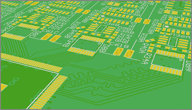
(Utilization of silkscreens in PCB production)
Accessory inspection
Classification of PCB may fall under rigid PCB or flex PCB. Rigid PCB is also divisible into three types: multi-layer, double-sided, and single-sided. You can further classify PCB into three quality classes: 1,2, and 3. Whereby under this classification, course 1 features the lowest requirement. The different PCB classes lead to PCB quality in inspection methods, complexity, and test. Multi-layered and rigid double-sided PCBs account for the broad applications in electronic products. Flex PCBs, on the other hand, are sometimes applied in exceptional circumstances. PCB inspection standards primarily come in several aspects:
- Standards made by countries
- Military standards depending on countries
- Industrial standards
- Inspection operations by device supplier
- Marked on the PCB design process design
Authoring tool file (IPC netlist)
The final part of the PCB manufacturing process is inspection and testing. The BOM features different files used for the last equipment inspection programming. Hence, you present the data in the same file with an IPC-2581.
The functional testing of netlist data is in the same file, and you can use the data to create test fixtures and programming test equipment. All extra information in readme files helps clarify the PCB data during the manufacturing process.
6. Things that CAM can help you/why should we use CAM
Using CAM has various benefits when it comes to the processing of components used in manufacturing firms. Compared to machinery manually operated, CAM offer:
- Multiple electronic formats
- Convert smart data
- Improve design manufacturability
- Verify the grid function
- Increase productivity
- Provide essential manufacturing and testing tools
7. Consequences of skipping a CAM test
Testing is vital for PCB assembly. Without intense testing, an entire PCB circuit board can fall apart in more than one way. Having your product fail in the field at the wrong time may have disastrous outcomes for your firm. Here are some of the common malfunctions when you skip a CAM test;
- Increase the chance of errors on the silkscreen
- Increase cost and quotation
- Avoid some sharp angles.
CAM systems are also as critical to manufacturers as their powerful equipment. Machinery shops worldwide are reaping the benefits of excellent CAM software beyond resourcefully programming their machining jobs. Operators can, therefore, structure their workload, set toolpath, and stimulate functions making the job easy. There are some design limitations for a CAM enabled machine-like.
- They are designed for a particular task and are not versatile.
- Require a skilled operator, programmers to run
- They also need an upfront investment.
However, once in place, they will potentially save you time and efficiency, increasing costs, and saving you thousands.
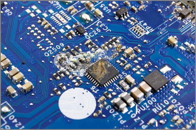
(You will likely face defects when skipping CAM test)
Summary
Our expert design solution will work with you to select the best PCB and CAM systems and implement them to match your unique environment. Our goal is to benchmark what we do by improving our service, process, and procedures.
We are scaling new heights, building our strength and trust while earning tremendous satisfaction from our client list worldwide. Our passionate, dedicated team of experts is the main reason for our success. We will improve collaborations between PCB domains and maintain connectivity through the electronic hardware systems.
