Printed Circuit Boards or PCBs are the heart of every electronic piece of equipment. You may want to manufacture a PCB for your DIY project or need high volumes of circuits for your business. In any case, you have to partner with a PCB manufacturing company that will get the job done. But do you know there are several considerations to make in PCB manufacturing service?
Asking questions is crucial to ensure a functional and high-quality batch of PCBs at the end of the manufacturing service. In this article, we will talk about the top 10 questions to consider for your WellPCB. We will provide you with a one-stop service and high-quality products. You can send us the documents you need to make and get a quote immediately! What are we waiting for? We have ten years of PCB manufacturing service.
Contents
1. PCB Manufacturing Services–PCB Design and Layout
It would help if you designed your PCB, considering many considerations before you can manufacture them. The first stage involves preparing a schematic of the PCB and uploading it to a good PCB signal integrity evaluation during PCB design because rectification may be complex after manufacturing. Use reliable PCB design software to complete the design. You can use different PCB design programs such as Eagle, Altium Designer, Circuit Maker, AutoCAD, etc. Now we are going to explore the critical questions that come up during this stage.
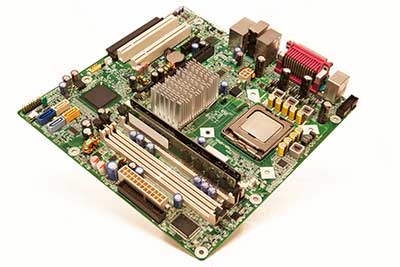
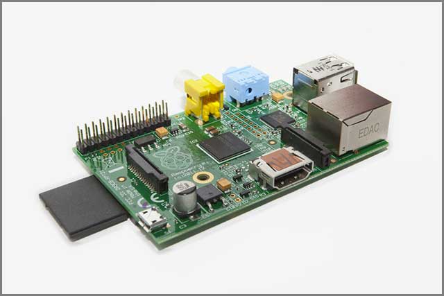
Printed Circuit Boards or PCBs are the newest revolutions in electronics. They are made of fabricated plastic with copper tracks in place of conducting wires. It makes these circuits compact and convenient to use than hand-made breadboards. The components of a PCB are soldered to provide it extra sturdiness.
PCBs, ensure safety since there are minimal chances of short-circuiting or wrong wiring. Computer-guaranteed precision in the production of PCBs is a significant reason to opt for them.
Here are the top things that a circuit board manufacturer can do for you:
·Standard PCB
An essential yet effective product by Printed Circuit Board manufacturers is standard PCBs, employed in a range of industries like telecommunications, security systems, audiovisual equipment, LED displays, process control, traffic signaling systems, lighting, et cetera.
Depending on your requirements, these manufacturers can offer single, double, or multilayered (up to 24 layers). You can also find specialized quick turn prototyping for all standard PCBs at competent Printed Circuit Board manufacturers.
·Metal Clad PCBs (MC-PCB)
LEDs are rapidly replacing conventional lighting alternatives as they are most cost and energy-efficient. The only drawback of LEDs is that they generate a lot of heat upon usage. Standard PCBs cannot handle this heat. Here come metal-clad PCBs that specialize in heat dissipation and can increase the longevity of LEDs.
1. How Can You Ensure an Errorless and Accurate PCB Schematic?
Designers use the schematic to state the function of the PCB and determine the placement of components. A proper and error-free schematic is crucial for the appropriate functioning of your PCB.
You should make sure to choose the appropriate PCB panel size. Many designers forget that they have to select a board size that meets the requirements of the equipment. Proper board size will enable you to keep the traces to the required minimum length, prevent waste of PCB real estate and keep the cost of the materials low.
If you want to go for mass production, the specifications and design of your PCB should be optimized for it. A small-sized board may meet your needs, but it may not be suitable for mass production.
The electronic engineer should also choose the correct grid spacing to avoid any spacing problems. The parts of the PCB should fit in the grid as this prevents any malfunctions. You should look for alternatives or use custom-designed products if some components don’t work with the grid.
Another way to reduce errors is to use the Design Rule Check (DRC) of the PCB design software whenever possible. Many designers keep it for the last, which allows small mistakes and wrong design choices to accumulate. Designers should check each step applicable with DRC so that you don’t end up with a line of errors at the end of the design.
Using DRC frequently saves you from the trouble of going through massive changes in the end.
2. What are the Best Practices for Component Placement on a PCB?
All the components on a PCB have their designated spot. You have to choose the correct placement for all the details after considering many factors such as electrical noise, thermal management, and functionality.
Designers maintain a specific order to ensure proper placement. First, the connectors are placed, followed by power circuits and precision circuits. After that, the designer puts the critical circuit components ending with all other elements.
You should also identify the critical test points and the application components. They should be placed near the test points so that you can detect faults promptly.
Silkscreen printing also goes a long way to simplify the PCB manufacturing process and avoid extra work. You can mark the elements and connection direction, components, and functionalities so that the manufacturer has no problem identifying the different aspects of your PCB.
3. What Trace Width should You Use?
Trace width is an important consideration when you design a PCB. Traces are the copper lines that run all over the PCB and connect the different components and connectors. The traces in the PCB are made to allow only a specific limit of current before they get damaged.
When current flows through a trace, it starts to heat up due to the inherent resistance. The temperature will continue to rise with the increase in current, and after a point, the trace will burn out, making the board useless.
The minimum trace width you can use is 1.0mm/A. The width is suitable for common types of PCB, which use 1.0 oz/ft2 of copper.
You can also use a formula to determine the required trace width of your PCB. First, you have to calculate the area with the following formula-
Area[mils^2] = (Current[Amps]/(k*(Temp_Rise[deg. C])^b))^(1/c)
The value for internal layers according to IPC 2221 is-
k= 0.024, b = 0.44, c = 0.725
The value of external layers is-
k = 0.048, b = 0.44, c = 0.725
You can use the formula for up to 35 Amps of current, 10 to 100 degrees C rise of temperature, and 0.5 to 3 ounces per square foot of copper.
Now let’s cover the questions about PCB specifications.
2. PCB Manufacturing Services–Specifications of PCB
You will need to determine quite a few things about your PCB during the manufacturing process. We will tell you the differences and advantages of all aspects to make an informed decision.
4. How to Choose between Single Sided PCB and Double Sided PCB?
Single Sided PCBs
PCBs are found in a wide range of electronic devices and are meant to connect electronic components. You will discover conductive copper and electronic elements on one side and conductive wiring connections on the other in single-sided boards.
These are often used in many electronics like printers, cameras, calculators, and radios. Single-sided PCBs are extensively used because they have a primary and straightforward manufacturing process.
The PCBs are suitable for non-complex and low-density circuit designs and have a low cost of production because of their basic design. All of the PCB manufacturers can understand and produce single-sided PCBs.
The simple design of the PCB results in fewer manufacturing errors, and they can be produced quickly in high volumes.
Double Sided PCBs
The double-sided PCBs come with a top and bottom layer and are traces on two sides. You can use electronic components and conductive copper on both sides resulting in a crossover of the paths. These are suitable for high-density circuit design and do not need point-to-point soldering.
PCBs are difficult to produce because of their complex design. But they are in high demand for complex circuits used in higher technology equipment. You can find double-sided PCBs in vending machines, lighting systems, amplifiers, and vehicle dashboards.
The PCBs provide an extra layer to accommodate the components, and you have space for additional connections. You can also reduce the size of the board as both sides of the board are usable. That reduces the cost of manufacturing.
5. How to Select PCB Core Material?
The core or substrate of your PCB is the non-conductive base and provides strength to the entire board. You can use different types of materials for your PCB with their advantages and disadvantages. You should choose your material based on the result you need, application, environmental and other factors applicable to the PCB.
The material used for the core determines the performance and level of integration of the PCB. The material should be durable enough and provide regular performance. It would help if you also considered other thermal, electrical and physical factors such as flexibility, temperature resistance, dielectric constant, tensile strength, dielectric strength, adhesion, and so on.
Here are the most commonly used materials for a PCB-
FR-4:
It is by far the most common material used for cores of PCBs. The epoxy laminate sheet is reinforced with glass to provide extra strength. The ‘FR’ in the name means fire retardant, and the material is also water-resistant. You can benefit from an excellent strength to weight ratio of FR-4.
PTFE (Teflon):
PTFE is ideal for high-frequency and high-speed applications as the plastic material offer no resistance. You can also use it for equipment with tight tolerances because of its flexibility. Various industries use PTFE in their PCBs as it is very lightweight and also fire resistant. The advantages of PTFE include versatility, material strength, and temperature stability.
Metal:
Some applications require the use of metals such as iron, aluminum, and copper. The material is ideal for Surface Mount Technology (SMT) and comes with mechanical durability. You can get along product life in metal PCBs.
Now we will discuss the considerations of PCB surface finish.
3. PCB Manufacturing Services–PCB Surface Finish
6. Which Surface Finish is Suitable for PCB?
A surface finish is applied to the PCB to protect the copper circuitry and ensure proper soldering. Selecting the right surface finish is essential for the successful assembly of the electronic components.
Currently, Electroless Nickel Immersion (ENIG) has become a popular surface finish. It is lead-free and suitable for complex components like flip chips and BGAs. The double-layered metallic nickel finish is costly as it uses gold to protect the nickel.
HASL is widely used for its low cost and durability. But it often leads to uneven surfaces which are not suitable for complex surface components. HASL can also be lead-free and repairable.
Organic Solderability Preservative (OSP) is a water-based organic finish used for copper pads. The environment-friendly solution is not as durable as HASL.
You can also use immersion silver which can be an excellent alternative to ENIG. The material is ideal for flat pack coating and fine pitch but can be expensive. Immersion tin is also available for the finish and is suitable for fine pitch products.
We will now find out more about PCB assembly.

4. PCB Manufacturing Services–PCB Assembly
The Bill Of Materials (BOM) of a PCB gets fitted onto aboard. PCB assembly process involves placing the electronic components directly on the board. You can use both manuals, and automatic procedures, so let’s find out more.
7. PCB Manufacturing Services—Which PCB Assembly Process should You Use?
Manufacturers use different methods to assemble PCBs, and the two major ones are Thru-Hole Technology (THT) and Surface Mount Technology (SMT).
THT
Components that end with a wire or lead can use the THT to assemble the PCB. The vias or holes in the PCB allow the information or wire to pass and then be secured with solder. Capacitors, coils, and other oversized items are suitable for THT as you can manually place them. Some manufacturers also use automated THT assembly processes.
At first, the components are placed manually or automatically on the board. A check is carried out to find any discrepancies and then passed on to an oven where solder paste is applied over the pins.
THT is not suitable for high volumes as the process becomes strenuous and time-consuming if done manually.
SMT
SMT is suitable for mass production as machines do all the work. It is also ideal for small components which have pins or terminators instead of lead or wire.
A stencil takes care of the soldering, after which the components are attached at the soldered points. A machine is then used to pick the pieces and place them delicately on the PCB. Next, the solder paste is passed through an oven to make it hard to secure the components.
8. PCB Manufacturing Services—How To Calculate Your PCB Assembly Cost?
Your Bill Of Materials (BOM) of a PCB get fitted onto aboard. PCB assembly cost depends on many factors. The labor costs differ according to regions- it’s far cheaper to make a PCB in China than in North America.
You have to factor in the turnaround time of your order. If you want a quick turnaround time, you may need to pay extra as the manufacturer may put off other work to finish your project.
The cost of production per board comes down in higher volumes and makes for an overall low cost. It may cost more to manufacture small batches of PCBs. You also have to factor in the technology in use- SMT is cheaper due to its automation, while THT costs more.
Now let’s head to the last chapter.
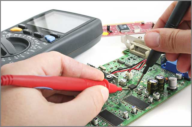
5. PCB Manufacturing Services–PCB Testing
9. How Can You Ensure Proper Functionality of PCB?
Many tests need to be carried out to ensure the functionality of the PCB. The significant tests are isolation and circuit continuity tests and determine the quality of the manufacturing process.
The circuit continuity test looks for any disconnection in the circuit, while the isolation test is done to determine any shorts.
You can also perform other tests like the “bed of nails” test by attaching springs to the test points. Then 200g of pressure is applied to them to test the durability of the test points.
10. PCB Manufacturing Services—What Quality Check should You Perform?
You can conduct a visual test of the PCB with a ruler and magnifying glass. Look out for any cosmetic defects like surface roughness or scratches and check the position of the pads.
Inspect the integrity of conductive patterns and find out if the vias are adequately punched. Test the coating quality and plating flux to ensure they are clear and firm.
Conclusion
Your PCBs will turn out just like the design if you consider all of the above questions for WellPCB. We will provide you with a one-stop service and high-quality products. You can send us the documents you need to make and get a quote immediately! What are we waiting for? We have ten years of PCB manufacturing services. It’s always better to be careful than just let the manufacturer decide things on your behalf. Asking the right questions results in the success of your project and higher profitability.
If you look for the right PCB Manufacturing Services, you need to look no more than WellPCB. We deal with PCB products offering highly specialized correct PCB service providers. Thankfully, there are various PCB Manufacturing services from China. Talk to our experts today to know more about how we can help you with everything from custom PCB to Assembly service.


