Contents
- 1 PCB Design Software
- 2 Some PCB Design Software Introduction
- 3 Some Best PCB Design Software
- 3.1 Kicad
- 3.2 Features:
- 3.3 For a free Kicad tutorial, let me show you now step by step:
- 3.4 PCB Design Software–Eagle
- 3.5 Eagle features include:
- 3.6 Altium
- 3.7 * Features of Altium designer include:
- 3.8 1. PCB Design Software—Altium Designer Schematics
- 3.9 2. PCB Design Software—Altium PCB
- 3.10 PCB Design Software–Diptrace
- 3.11 PCB Design Software–Pulsonix
- 3.12 User notes:
- 3.13 Sprint-Layout
- 4 Tips When Choosing And Using PCB Design Software
- 5 Make Your PCB Board Design Into Reality
- 6 PCB Design Software–Conclusion
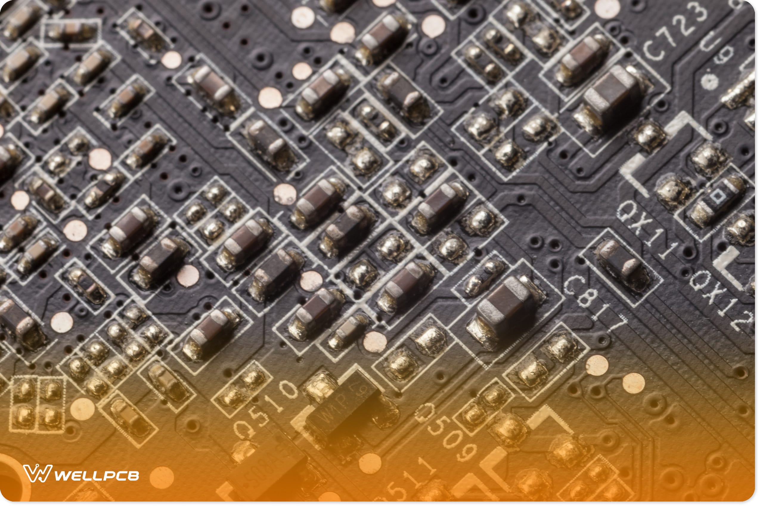
PCB Design Software
PCB signal integrity evaluation must be done during PCB design because rectification may be complex after manufacturing.
Use reliable PCB design software is a software suite for electronic design automation. It is a convenient way to design circuit boards with your creativity and computer animation.
manufacturing PCBs will work before production.
These software products are essential for any electrical engineer’s success.
Creating a PCB that handles a current load and gets the job done is only possible with a seamless design, which software can help you build with minimal frustration.
Therefore, you must find PCB design software that is easy to use and matches your needs. This guide will help you do just that.

Some PCB Design Software Introduction
Not all PCB signal integrity evaluations must be done during PCB design because rectification may be complex after manufacturing.
Using reliable PCB design software costs a lot of money. If you are on a budget, check out these free software options.
Some of the best software out there doesn’t cost a thing:
• ExpressPCB
It is excellent free CAD software that can benefit engineers or students who want to complete school projects for free.
It boasts a valid but limited library, which can crimp your creativity.
Another frustration is that it lacks rubberbanding to show the interconnectedness of boards, which is very important. It is helpful for visualization or student projects but little else.
They will consider Gerber files for an additional fee.
Though ExpressPCB boasts a small library and outdated programs, It is a valuable tool for learning PCB design, mainly if you are a student.
Its simple layout will remove the stress from learning as you experiment with PCB design.

• TinyCAD
It is the most straightforward free program available, and it gets the job done without bells or whistles. You can create any components missing in the library. You can also copy and paste your designs into a Word or .png file to save and print.

It is possibly the best free software option for beginners because it does not limit PCB size and allows you to create multiple pages.
However, it has a limited library and some dated components.

• DesignSpark PCB
It is an excellent free software that is soaring in popularity. You will enjoy the intuitiveness that makes this program so simple to use.
It offers designing, schematic capturing, and layout improvement for no PCB cost.

• PCBWeb Designer
PCBWeb ordering the parts you need is a breeze. It also has a smooth learning curve.
• Altium Designer(aka Protel 99SE and Protel DXP) (15-day Trial)
1. Required OS: Windows XP and a powerful computer at a minimum.
2. Description: Commercial electronics and embedded design package.
3. Powerful that includes:
- Schematic capture and library editor.
- PCB design and PCB library editor.
- Gerber editors.
- VHDL and Verilog (and probably more) hardware compilers.
- C to Hardware compiler.
- C compiler for different cores (ARM, Microblaze, Nios, etc.).
- Library generator that imports data from your company IC database.
4. Customer Feedback
Easy integration of schematic and PCB editors, as well as library editors.* User1: I have used this package primarily for schematic capture and PCB design.
I find manual routing quite comfortable and productive, with a powerful rules editor and control that help too much when placing tracks.
* User2: For all those issues related to clearances for mains and high voltages, currents, and so on, its ruled editor is helpful, limiting the manual routing when tracks reach the limits imposed. It may be overkilling regular users, hobbyists, and little companies. I found that I use probably <20% of all its features.WinAVR, AVRStudio, and FPGA free software are more than enough and can replace these other licenses.
It may interest you.* User3: For those who have not seen the new Altium pricing model.
I ignored their upgrade requests over the years since Protel99, as I did not see any value in their upgrades, but their recent special for a perpetual license for $2k changed my mind.
In China, the Altium Designer Software is widely used mainly in relevant university departments because of its powerful editor.
• gEDA
gEDA is a suite that gives you several open-source software in one. It will produce other file types, like .ps or .png.
With an auto-router and many other features, this software is robust and low-cost for PCBs. It is best used with a gEDA schematic editor.
It has a rich library and a professional support community for no extra charge. Many say you prefer gEDA to Eagle because it has fewer limitations!
It is mainly oriented towards printed circuit board design for electronic format released under the GPL.
It is a collection of open-source electronic design tools. They may be installed individually, but you get the lot by installing them.
It is mainly oriented toward printed circuit board design (as opposed to integrated circuit design). Its applications are often referred to collectively as “the gEDA Suite.”

1. Features
- gschem schematic capture
- gsch2pcb transfers information from gschem to PCB
- PCB for layout
- gerbv-Gerber viewer. Look at layouts
- calc-Transmission line and electromagnetic structure analysis
2. User notes:
- It can produce other file types like ps and png.
- PCB is one of the most mature packages, starting in 1990 on an Atari, and is the best free PCB tool.
- The application is feature-rich, straightforward to learn, and has no limitations like Eagle. It also blows doors over all the other packages listed here, IMHO.
- Most importantly, PCB does include an auto-router!
- PCB, used with the gEDA schematic editor, is a great combination: it is easy to use, has huge libraries, large worldwide online communities, works cross-platform, and has professional industry support. Many Aerospace companies use this suite, for example.
Best of all, gEDA and PCB are open and Exampleurces. I think they are even more comfortable than Eagle.
As a consequence of the project’s openness, schematic symbols, footprints, and utility scripts are freely created and shared amongst the members of the gEDA community at a spin-off website(gedasymbols.org)
Most PCB software offers a free trial, including OrCAD, Kicad, and Eagle. You can try the software, see if you like it, and then make a purchase decision.
• FreePCB
This is a free, open-source PCB design editor for Microsoft Windows. It was designed to be easy to learn and use yet capable of producing professional-quality work.
Its features include 1 to 16 copper layers, a board size up to 60 inches by 60 inches, the import and export of PADS-PCB netlists, and more.

♦User-notes:
- I created the last three boards for my low-vision barcode reader using FreePCB; in the first version, I used ExpressPCB.
- We have also sampled other layout software, such as PCB Artist (a proprietary program offered by Advanced Circuits) and the freeware version of Eagle (mentioned above).
- Use FreePCB and find it easy and intuitive to quickly create circuit layouts since it has a very short learning curve.
- It is mainly for the hobbyist because it doesn’t have many of the bells and whistles that circuit boards have.
- The top software includes PCB Artist, Altium Designer 17, Ultiboard, DipTrace, SOLIDWORKS PCB, PCBWeb, BSch3V, Gerbv, XCircuit, Eagle PCBs, KiCad, and others.
- In all these programs, I have always found the biggest hurdle to overcome to be the generation of and access to footprint libraries.
- Moreover, when I first began using FreePCB, it had a unique FOOTPRINT WIZARD! By inputting the package dimensions from the printed datasheet of your chosen components, the FOOTPRINT WIZARD created a custom footprint that could be saved in the “User” library folder and repeatedly added to your PCB!
- Additionally, you can toggle parts out of your board layout to make minor adjustments.
- When I begin a schematic, I usually print the pin-outs from the datasheet of the components I plan to use. I then cut out the layout with scissors and pasted it onto a large piece of drafting paper, penciling in the connections between pins. At this point, I go to my local print shop and have a copy made. From there, I lay all my traces by hand in FreePCB!
- If you are a novice, you may choose a local board house (like Advanced Circuits) that can help you configure the software to generate the CAM files properly.
- The terminology can be daunting, and most board houses will not correct your mistakes.
- However, the “free call back” service AC circuits offers is priceless for a novice!
Cons:
FreePCB does not include a schematics editor. You have to enter your netlist by hand!
Suggest that newbies to PCB design read the Getting Started doc; it has a super introduction to the
The PCB designing process is often overlooked by manuals (which assume you have some idea of what you’re doing).
What do you, other users, use for schematic entry?
How is the autoroute package?
Some Best PCB Design Software
If you are trying to select the best software to use, consider these three excellent options that we strongly endorse:
Kicad

Kicad is accessible and user-friendly software. It allows you to create schematics and convert them to PCB designs.
Besides, it works to generate Gerber files, bills of materials, artwork, 3D views of a PCB, and various other components.
Features:
1. It can help you to design a circuit that can automate your house
2. It can also facilitate building a camera add-on for a quadcopter.
3. It can also help create a compact and unique alarm system.
It has five parts: KiCad, Eeschema, PCBnew, GerbView, and Bitmap2Component.It features Eeschema. KiCad uses the integrated environment for each stage in the design process: PCB layout, Schematic capture, Gerber file generation/visualization, and library editing.
It works as a cross-platform program. The language is C++ with wxWidgets. It sprints on FreeBSD, Microsoft Windows, Linux, and Mac OS X.
There are availabilities of several component libraries, and users of the software can also add other custom components.
Ideally, it is helpful for house circuits, camera add-ons for quadcopters, and alarm systems.
The best part is that it has the lowest PCB cost and features that make EDA easy.
It is very affordable, and WellPCB offers DC motor controllers in domestic and international markets. We are flexible when it comes to designing electronic circuits.
Also, installation is straightforward. Immediately, you get your computer connected to the internet and running Linux.
Kicad comes with the symbol and 3D model libraries. You can also add your libraries. Download footprint libraries from GitHub.
For a free Kicad tutorial, let me show you now step by step:
• Step 1: Downloading Kicad Tutorial
The first thing you need to do to get started is to download KiCad. Depending on your program, you must contact the latest version of your software.
Once the program has been installed, you need to create a navigation window allowing you to open peripheral programs such as manufacturing PCBs; there are high chances of layout failures, which can negatively affect the final product’s functionality. There are several PCB layouts and schematic capture.
• Step 2: Setting Up the Project
You must download the KiCad design and unzip the files in your local directory. The files that may be needed for this purpose include:
Pro – to help keep track of the structure
CMP: defines the footprints to be used with schematic components
Kicad PCB manufacturer, then the process is more hectic. They will design the PCB layout: they represent the PCB layout
Sch- refers to the schematic
These main files need to be shared on a KiCad design. You may also need to share the footprint file.
Notice that KiCad works differently from Eagle and requires you to define each component’s footprint.
• Step3: Setting Up the Component Library
It would be best if you double-clicked on the Kicad Schema. If you get an error, ignore it. If the schematic loads with a question mark, it shows that KiCad is missing the link, so you may need to link it to the devices containing the schematic.
Linking Your Components to the Libraries
Click on your component libraries and allow the creation of an open window. The project file has information about where the component library file is located.
• Step 4: Adding Components to Your Schematic
If you want to add a device to your schematic, click add. This opens the component window, where you can choose a component from the hundreds of features available.
The next thing you need to do is select the device and press enter. Then, please place it in your following schematic.
Once the capacitor has been placed, it will still be in placement mode. It would be best to hit Esc to return to normal pointer mode.
Copying the component is easy; just put the mouse at 3.3v and press c to help duplicate the device and place it in the required position.
• Step 5: Wiring the Components
You should then wire the components together by placing the mouse pointer over the bubbles and pressing W.
• Step 6: Annotating the Schematic Components
KiCad helps to auto-annotate your schematic. Here, you should click on annotate the schematic components button, use the default setting, and click to confirm it.
Kicad will request that you verify the annotation. Once you confirm, the components will be added.
Is Kicad better than Eagle?
Many electronic designers want to know. However, the truth is that both programs are excellent and will offer you what you need.
The best part is that Kicad is the cheapest option, lowering your overall PCB cost. Eagle has a free version that is more limited than Kicad.
Kicad also has more keyboard shortcuts to reduce your work with your mouse and save time and wrists.
You can download Kicad for free.
You must select your operating system and follow the on-screen directions.
PCB Design Software–Eagle

“Eagle” is often used by professionals. It stands for “Easily Applicable Graphical Layout Editor.” Its simple user interface makes it excellent software with a fantastic schematic function.
It also offers copper cladding, batch command execution script files, and online positive and negative annotation functions.
While there is a fee to use this software, many find it quite affordable.
Eagle features include:
1. An auto-router
2. Modular schematic editor
3. PCB synchronization
4. Schematic Rule Check
5. Object alignment tools to help align your work
6. Design check ruling to customize PCB rules and restraints.
7. Copper pouring
8. Different types of outputs for manufacturing data.
9. Routing at advanced levels.
10. Differential pair routing technique.
11. Backward and forward annotations between printed circuit boards and schematics.
12. Users can define certain things, such as the clearance, nets, and widths of wires.
13. Can run on any computer, from PC to Mac.
14. Community support
15. Lightweight uses 50-200 MB of space, and the downloader uses 25 MB.
For a fascinating Eagle tutorial, please go here.
You will learn how to use this software to create fantastic circuit boards with the intuitiveness and creativity you desire and how to merge multiple into one.
Also, learn how to export Gerber files here.
Many users enjoy the Eagle PCB design full version free download crack. Upgrade to the more powerful version for just $15 a month.
To download Eagle, please visit here.
So, how does Eagle compare to Altium? Eagle boasts many features with a lower price tag. However, it lacks an autorouter, simulators, and 3D viewers.
However, Altium is easier to use in many states, though both programs have a steep learning curve.
Eagle is generally best for designing beginner to intermediate PCBs who don’t want to fork out much money.
Benefits of Eagle:
•You can quickly learn and master the Eagle PCB software.
•It is designed with flexible, user-friendly language programs, which makes them easy to use. It can easily export the Gerber files, which you can use on any other board.
•It approves of the differential double routing and meanders. It ensures that all the necessary connections are made adequately through the Design Rule Inspection.
•The Eagle PCB supports the personalization of schematics and sheets by using descriptions.
•The schematic is then controlled by using the ERC, otherwise known as the Electrical Rule Check.
•Eagle PCB fully supports sheets and complex designs. This software can easily create a circuit board with a single mouse click.
•It can also schedule schematic sheets via Drag & Drop. Eagle PCB software can easily take care of all kinds of assembly variants.
•With this software, you can easily use a dimensioning tool. It also approves multiple layering.
•Eagle PCB enables the BGA escape routing automatically. The router of the Eagle PCB will save you time.
Altium

The Altium Designer is an excellent PCB signal integrity evaluation tool. It must be used during PCB design because rectification may be complex after manufacturing.
Use reliable PCB design software that will help you create stunning PCBs for multiple real-world applications. It is mighty and requires Windows OS to run. Some of its best features include:
* Features of Altium designer include:
1. A high-quality 3D visualization that allows for routing using 3D.
2. The automatic appearance of net names on the pads of the printed circuit board editor.
3. Outstandingly advanced filtering simplifies the selection and modification of what a user wants.
4. A simplified design constraints creation procedure that has an inbuilt helper.
5. Manufacturing and Generation of the output file are superior, and its settings are easy to configure.
6. A good number of hotkeys and shortcuts allow PCB design efficiency.
7. Its design system operates offline and can still function without a license.
8. The add-on for export and import used in other programs and formats is quite decent.
9. Its simple project tree allows users to drag and drop files to desired locations.
10. Library generator that imports data from your company IC database.
Also, a variety of free software within Altium usually makes it unnecessary to purchase other features. You get what you need to be included in the overall package. There is integrated debugging and simulation of VHDL, synchronizing PCB, FPGA, and signal integrity designs.
The Altium Designer software is the most famous and user-friendly platform for the design engineer to draw schematics and do PCB layouts.
This software has all the necessary tools to design state-of-the-art PCB layouts professionally.
Here, we will discuss the options available in Altium schematics and PCB design.
1. PCB Design Software—Altium Designer Schematics
The Altium schematics have a detailed version of the library of components available.
It has so many renowned component manufacturer libraries.
Design – Browse Library
Most passive and active components generally used in every electronic circuit can be found in “Miscellaneous Devices.”
Design – Browse Library — Miscellaneous Devices
When we select any component through-hole or SMD, the corresponding footprint will appear in the library pane.
We then click the “Place” button on the library pane/window to place the element on the schematics sheet.
After we double-click the component, we will get the properties window of the element, as shown below.
Then, we click the Add button to add the component’s footprint.
Add – Browse – Misc Devices
This new window will show the details of the PCB footprint of the component (details about the SMD size and 3D model). In this way, we can change the footprint of the selected element as per our requirements. For example, we can find the exemplarity of the commonly used impression in the different devices, like SOT-223-4N.
This footprint is widely used in medium power transistors and has four leads with a tab connected to the body as the heat sink.
We can also edit the pins of the Integrated Circuit placed on the schematics by double-clicking the component.
Component Properties – Edit Pins
The pins available are Input, I/O (Input / Output), Output, open collector, passive, high Impedance, open emitter, and power. The VCC, VDD, VSS, and GND are all power pins. The bidirectional input/output are IOs, and so on.
We can also create a user-defined Component library in this way
File – New – Library – Schematic Library
The component can be designed using rectangles and circles to create a notch in the IC. As discussed above, we can also place as many pins as required, give them names, and define their nature.
2. PCB Design Software—Altium PCB
We can pan on the PCB layout board by holding the right click and moving the cursor around the screen.
We can switch the PCB layout from a 2D to a 3D view and vice versa. The schematics-generated netlist can be imported to the PCB layout board to draw interconnections/tracks/routes.
The routing can be done Auto or manually. PCB Rules and constraints can be set.
Design – Rules
Clicking the PCB layers switches them ON and OFF. Double-clicking the layer “LS” opens a window with a detailed layer configuration.
The PCB Preferences give all the details about the PCB Editor.
Altium thus makes integration easy and a powerful rules editor and controls to assist in placing tracks. Ultimately, it is everything, Eagle and more.
The Altium viewer offers 3D viewing, which makes it possible for you to cluster several nets to one signal, supports rigid and flex designs, supports custom overlay, adds the hole tolerance, and allows dynamic display where the clearance of boundaries when routing.
Finally, a release and data management tool allows you to format Gerber files.
You can create and save templates and track designs and changes through ECO.
Cloud publishing keeps you in case you ever suffer from a hard drive crash and gives you more freedom to work on multiple devices.
The libraries in this software are robust. You can customize them and find all the components that you would need to include within them.
The schematics feature many renowned manufacturer libraries.
For a full Altium design tutorial, visit here. This tutorial will show you how to use and export Gerber files on this software.
Altium is not free. You will have to pay $2000 for a perpetual license. It’s the highest PCB cost, but since this product benefits even the most advanced designers, most users say it is worth every penny.
PCB Design Software–Diptrace
Diptrace is a way to save time by efficiently and quickly creating designs without a lot of headaches. Ideal for beginners or time-crunched individuals, It allows you to develop other schematics and convert them to any format, such as PCB.
It offers flexible features like 3D modeling, high-speed shape-based routing, and extensive import/export capabilities. While switching from one form to another form, it also assembles the electrical components. It offers multi-sheet and multi-level hierarchal circuits.
There are four modules within Diptrace.
These include schematic capture to connect pins without wires, schematic conversion, and import and export from other CAD or EDA software and formats.
It creates greater versatility for how you can use this software.
The PCB layout tool affords much greater flexibility in board design. It features intelligent manual routing of high-speed and differential signals.
The verification feature lets you quickly check the accuracy of a complicated project accuracy using virtual high-speed signals.
It contains one more helpful tool, real-time DRC, which can be used to fix errors and enhance the quality of the project until it compiles.
This can be used to create 3D models and to build and expand your Diptrace library as you see fit.
There is also a component editor that lets you manipulate components.
That defines electrical pin parameters for you and attaches the patterns to 3D models.

What makes Diptrace so great is its simplicity. You can create patterns of different dimensions and shapes. Even allows for export features and real-time 3D review.
Displays models of the manufactured printed board and the installed components.
It allows you to rotate the board, zooming in and out as you please.
It also allows you to change the colors of everything, including the background.
PCB Design Software–Pulsonix
It’s an easy-to-use, complete professional package with an excellent (optional) auto-router.
Pricing starts at $1750 for a basic 1000-pin version.
That might seem expensive compared to other products like Eagle, but it is excellent value given that designs can be completed in a fraction of the time they take with Eagle.
Pulsonix combines schematic entry and PCB layout in one program. It is fully compatible with Windows standards and was developed using OOP techniques from the outset, making it easy to add new features and fix problems without introducing additional bugs.

User notes:
- Schematic entry is very intuitive – select the parts needed from the libraries (a preview of the schematic symbol and PCB footprint is provided), place the elements, and connect them. Unlike Eagle, the pins don’t have to be on the current grid to be correctly connected; the connection ‘jumps’ to the nearest pin, if necessary.
There is a beneficial electrical rule check that identifies anomalies, such as unconnected pins, unfinished connections, and so on.
Components that need to be close together can be ‘grouped,’ and the groups are carried forward to the PCB.
- Part creation is straightforward, with pin and gate swapping. Nets can be assigned to pins in the part editor, and unconnected pins are allowed. This avoids clutter on a schematic by not showing the power connections. Net types can be defined for each pin, including no-connects, making it very easy to avoid silly mistakes in the design.
- Pin names and numbers can be copied from data sheets and pasted directly into the part editor of Pulsonix, saving much typing. FPGAs have unique requirements and are supported. Excellent reporting facilities are provided, and user scripts can be defined as a particular BOM format for custom reports.
Wizards are provided for creating footprints and schematic symbols for virtually every type of part, including BGAs. Pads of any shape can be created manually if required.
- Schematic and PCB designs and part libraries may be imported from most other popular packages, including Eagle.
- I used it for over 20 years. A particular version of Easy-PC is available.
Overall, it was like Easy-PC with the interactive auto-router features I wanted. It also has 3D models, import, and exportability, typical of a mid-range package.
However, I liked that Copper Pours worked adequately (unlike Altium), the user interface was straightforward, and I didn’t run into weird random bugs.
Sprint-Layout

Sprint-Layout’s logical and straightforward layout makes it ideal for anyone, particularly those in a hurry.
There is no unnecessary “ballast,” making it challenging to keep the overview or almost impossible usage.
Sprint-Layout has tools to draw pads, tracks, copper areas, labels, etc.
With Gerber and Excellon’s support, it can be possible to use this for professional manufacturing.
However, you can also print out your designs with this software.
Selecting the corresponding mode allows you to place your elements and all parameters, such as track width and pad size.
They are always available and can be edited at any time. A CNC machine can also create HPGL files for isolation milling.
The only notable cons include non-integration between the PCB layout and schematic design. The auto-router also has some complaints.
The logic of the layout may make this worthwhile for you, however.
Tips When Choosing And Using PCB Design Software
When selecting a signal, integrity evaluation must be done during PCB design because rectification may be complex after manufacturing.
Use reliable PCB design software; you need to keep a few factors in mind by asking yourself these questions:
1. What level of design are you looking for?
2. Do you need multiple pages?
3. Do you require auto-routing?
4. How much are you willing to spend?
5. What kind of computer system do you use?
6. How much space do you have?
7. Are you happy that working Custom PCB may be a tall order?
Will this article teach you five basic ways to land the best online PCB board?
Alternatively, do you need an offline program?
8. Do you want to create or buy components or have a very robust library to choose from?
Be sure to consider these things.
Then, review the software to see which meets your specifications.
You must find one on your operating system that meets your RAM specifications.
If you can’t always work online, an online system may not be ideal.
Bear in mind that free does not necessarily mean free.
Sure, the software won’t take anything out of your pocket, but challenging software with lots of free glitches or limitations can pose more than a hardship than it is worth.
Especially for new users, a support community can be beneficial.
You will have questions – it is inevitable when you are starting.
Reading the tutorials and tips of software veterans can help you discover tools or features you didn’t even realize existed within your chosen software.
Also, be sure to research the software you consider before using it.
Read user reviews and look at screenshots of the work performed on these.
Ask if each software meets all of your needs. Do the final products look the way you want yours to look?
A good idea is to try different software trials to determine what you want to use as your go-to software.
Free software can help you learn to use PCB signal integrity evaluation during PCB design because rectification may be complex after manufacturing.
Use reliable PCB design software adequately and learn what limitations frustrate you to search for programs that don’t have those limitations.
Watching online tutorials on YouTube can also help you understand how the software works before you use it and find out whether you like it the hard way.
Make Your PCB Board Design Into Reality
Now you have learned many of the pros and cons of different PCB signal integrity evaluations during
PCB design because rectification may be complex after manufacturing.
Use reliable PCB design software programs. You can’t wait to try them out to begin your EDA adventure. Your life will certainly change now.
To make your designs a reality, now it is time to find a reliable and professional PCB manufacturer.
WellPCB is an excellent place to start with our affordable yet high-quality products.
Get a free instant quote to your specifications today.
With our Bartels auto engineer, you can find products that meet your needs exactly. Just fill out the product specifications boxes and submit for a quote.
PCB Design Software–Conclusion
You have the keys to finding the best PCB signal integrity evaluation. This evaluation must be done during PCB design because rectification may be complex after manufacturing.
You should use reliable PCB design software, and you should also know how to use this software to its fullest potential.
Please contact us today to quote PCB assembly turnkey services or read great articles on PCB design.
Check out our helpful items and fantastic support team to assist you with your PCB design needs.