On Copper PCB, Several possible problems can occur with a PCB, but you can say there are just four common causes that lead to PCB failure:
1. Burnt Components.
2. Poorly Manufactured Components.
3. Environmental Factors.
4. Age.
The copper PCB is mainly used because it solves or reduces the regularity of these failures; with the wood and glass PCB, you have to make sure the soldering iron temperature is more or less perfect as any higher can lead to a Burnt Component.
The Copper PCB is one of the most accessible PCB to make as the materials needed and the assembly service that makes it readily available. We at WellPCB can reduce PCB problems to as low as possible, eliminating such things as Burnt Components, poorly manufactured components, and age.
So, how to assure or make it ideally from each aspect, let’s see whether this guide shows us what to do.
Contents
1. Copper PCB—Copper On PCB
Copper PCB is the most used of them all based on its Electrical conductivity and Thermal resistance. PCBs with a copper structure (copper-clad or foil) on top of the reinforcing material.
Or has copper as the primary material because of its conductivity. Copper PCB is favored among engineers because of its adaptability.
People are choosing Copper PCB because of several factors like:
1. It’s increased Thermal conductivity, which in turn spreads out the heat across the board, significantly reducing the chance of a burnt component
2. Its increased Electrical conductivity
3. Potential to use the material to its fullest (You can use every space without considering thermal and electrical repercussions)
4. The possibility of another copper coating.
You don’t need much consideration when picking copper PCB. You can use the copper PCB from a talking teddy bear toy on your TV remote, provided you have in-depth knowledge of electrical engineering.
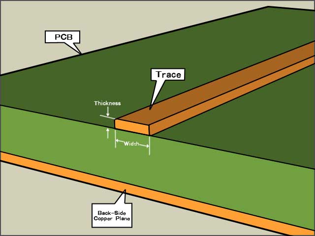
Depending on the type of PCB (single, double, multilayer, rigid, flex, or rigid-flex), the thickness, and the weight change, there are standard sizes for a range of electronic products.
As said previously, a PCB aims to make sure there is a steady flow in the circuits. As such, things like weight and thickness are significant factors as they technically change the entire handling of a PCB, from the type of solder to the soldering iron, the soldering technique, and the temperature you need.
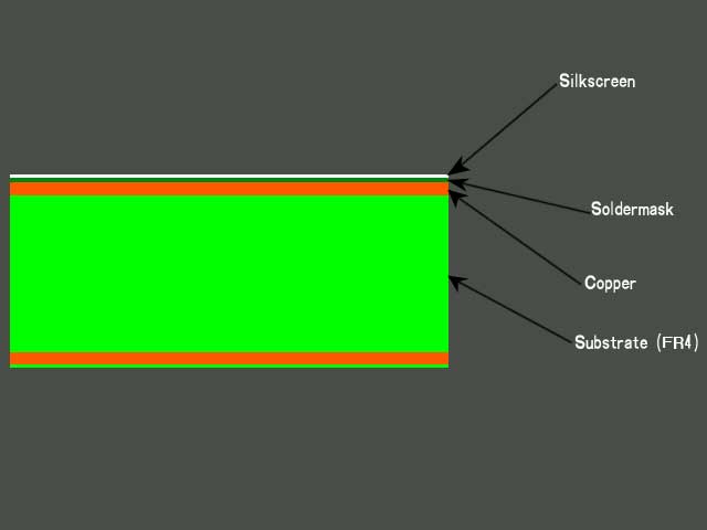
The composition of a copper PCB is majorly made up:
1. Silkscreen:
This is also called screen printing, a printing technique used to add ink(primarily green) on the substrate as a painting in terms of the PCB.
It is used to show things like the letters, numbers, symbols, and imagery (power inlets and outlets, potential microchip placement, transformer location, plus+, and negatives- ) on the board. Usually, only one color is used, and visibility is generally relatively low.
2. Copper PCB—Soldermask:
This is the second layer on a PCB. It is the pseudo shiny finishing layer of polymer that is on the copper traces of the board.
Its job is to protect against Environmental factors like oxidation and dust or debris from gathering in between the solder pads. A solder mask also helps prevent what we call a solder bridge. A solder bridge occurs when there is a slip while using the soldering iron, causing two conductors to contact.
3. Copper:
The Copper gives the PCB its excellent high performance. It provides the PCB material its surface roughness and when the copper is combined with the dielectric material.
The two work together to give the PCB its excellent performance output, especially in RF and Microwave frequencies.
The copper shows the signal pathways on a PCB, the circuit patterns you see are made with high precision that only copper with high quality; when combined well with the PCB’s substrate material can produce it.
Copper has a coefficient of Thermal Expansion (CTE) of about 17ppm/°C, which is the amount of expansion and contraction that the material undergoes when the electronic device commences work.
4. Copper PCB—Substrate:
The substrate in the underlying layer, board substrates, are usually dielectric composite materials, mainly composed of epoxy resin and reinforcement (glass fibers, sometimes woven or nonwoven, and even paper has been used).
With the resin, filler-like ceramic is known to be used. The most common type of substrate is the FR -4 (where the FR stands for Flame retardant); the reason you can say the FR -4 copper is the best is because of the excellent conductivity feature that makes it stand out even among the fiberglass substrate.
Another feature of the FR -4 copper is its high strength, dielectric properties, and apparent thermal resistance. The melding of copper and the substrate is paramount to the performance and reliability of a PCB.
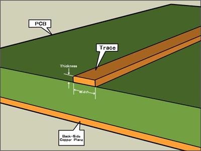
2. Copper PCB Thickness
As previously mentions, you need to always consider the thickness and weight of a PCB before use.
YES, a copper PCB can take a lot more thermal resistance and electrical conductivity; it doesn’t mean you use a PCB meant for your beepers on a supercomputer; that’s like trying to catch a fish with just the line and no hook or bait; A CERTAIN FAILURE.
2.1 Copper PCB—Copper Thickness Unit
The standard copper unit of measure for its thickness is Oz. (ounces). However, it can be measured in Inches. Most times, people don’t consider the thickness of the copper regarding the PCB, but the thickness of the entire PCB after the 1oz copper has been pressed flat and uniformly spread across a 1 square foot area.
Nearly all printed PCBs are built with 1 oz copper thickness. When it comes to PCB manufacturing, manufacturers assume 1 oz. They are quoting and constructing the design unless the customers provide particular specs.
A customer has decided that the design needs additional current than 1 oz, can carry, then increasing the copper width or your traces width would be better. In some cases, finished copper is one oz.
More significant than the starting copper on external layers, but when it comes to interior layers, finished copper is equivalent to the starting copper.
Usually, 2 oz. 1 oz copper thickness is undoubtedly the most familiar and standard copper weight since it often gets to the point of not being neither excessive nor too little. Copper thickness is excessive and more costly, while 0.5 copper may not be adequate, particularly for ground planes required to endure higher currents.
As such, 1 oz copper thickness is often the most suitable option to match your design and financial needs.
In case you need tighter trace plus space, you should generally do; duplicate the layer that needs heavy copper and ensure that you cut the copper into two. Supposing you need eight mil lines plus 4 oz copper, the best option is to duplicate the layer and use 2 oz. Copper.
For starting copper weights weighing 5 oz. or more, doubling a layer is also recommended instead of thicker copper. It is cheaper to add layers than to use thick copper when the processing complexity of the thicker copper is considered.
To put it another way, a 2-layer, 6-ounce copper board usually is costlier than a 4-layer, 3 ounce one.
2.2 FAQ About Copper Thickness
The first question most customers ask is based on the BAC-Final-Web-107Minimun line breadth capabilities of a PCB manufacturer. However, in most cases, the copper weight is rarely the answer.
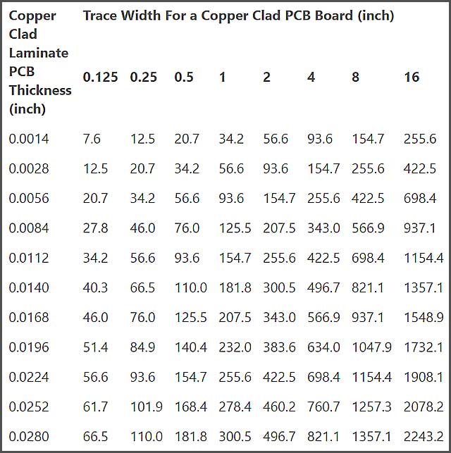
The table above shows the copper thickness about the width.
3. Copper PCB—Copper PCB Weight
We have talked about the importance of the Copper PCB thickness; now, we will take an in-depth look at why the weight of a copper PCB is as significant as the thickness.
The weight of a PCB by default is always around 1.2 oz. of copper, with a one 0z. The copper thickness and one mil copper in plated through holes.
|
Ounce |
Grams |
Micron |
| 1 | 300 | 35 |
| 2 | 600 | 70 |
| 3 | 900 | 105 |
Of course, the base ranges from 0.5oz. To 3.0 oz. At the same time, the plated copper ranges from 0.7 oz. to 2.0 oz. The higher the weight of the copper, the better the electrical properties and the more complex the etching process on the board.
You should know the weight is significant has it affects many things about the PCB like:
1.The achievable trace and space width dimension
2. The least widths suggested for annular rings
3. The base copper determines the amount reduction needed on the line, so the more the base copper equals, the more the line reduction.
Much attention is paid during PCB design phase that could make or break a PCB especially when the weight of the copper that you want is not stated:
1.Pads that are not functional on the inner layer
2. The short-circuiting can be avoided by giving tolerance to the edges
3.Aim for a minus tolerance on the small holes
4. Always factor in the thickness of the copper. Most times, that is just 1 oz. of copper.
3.1 Development Of Heavy Copper Advanced PCB
In developing heavy copper with advanced PCB, multilayer PCB is produced using copper layers ranging from 2 to 5 layers of copper at different levels. Which is interconnected by using similar layers of copper?
The additional copper level enhances the board’s functionality, and extra vias help in passing more current PCB by keeping the pads well attached. It helps improve the strength of the residence to hold the bolt by maintaining the required cable in place.
New low-cost manufacturing has also been developed, which provides necessary assistance to the assembly by replacing heavy copper protruding up to twenty miles off the surface.
The buried technology used in heavy PCBs can have any amount of copper above the surface or below the board’s surface.
3.2 Assemble A Higher Current PCB And Heavy Copper-Based Board
When we assemble a higher current PCB and heavy copper-based board, it could be challenging to develop but not impossible because it needs extra time and effort.
To develop such a board, extra care is needed from the engineers to design and develop the board by observing the transfer of heat in the form of thermal transfer.
PCBs with heavy copper need to be soldered using the high enough temperate and soldering it correctly for better results. It is highly recommended that the manufacturing of the PCBs by using the higher level of temperature lead-free.
Would laminate it properly to help in keeping the pads attached with all the retained heat.
WellPCB. We will provide you with a one-stop service and high-quality products. You can send us the documents you need to make and get a quote immediately! What are we waiting for? We have ten years of PCB manufacturing has become the most crucial option in China for those who are the starter or experienced in manufacturing PCB. People involved in this manufacturing could supply the essential features to their customers in foreign countries.
By adopting an excellent option of selecting preferential shipping agent.
WellPCB. We have ten years of PCB manufacturing in China, which has gained momentum due to cost-related issues. We will provide you with a one-stop service and high-quality products. You can send us the documents you need to make and get a quote immediately! What are we waiting for? Because manufacturing PCB in China has lower costs in comparison to other regions of local manufacturers.
You can take services from WellPCB because they are reputable manufacturers in China. They are offering their services to their customers from small to large scale WellPCB. We will provide you with a one-stop service and high-quality products. You can send us the documents you need to make and get a quote immediately! What are we waiting for? We have ten years of PCB manufacturing.
To place your orders, you are advised to browse their website and submit the desired information through Gerber files.
You are advised to specify what types of customization you need in your PCB manufacturing because we have experience in offering excellent options to the customers to develop the customized PCB assembly for you at an additional price.
The company has experienced resources available to ensure you get the best value of your money invested with us.

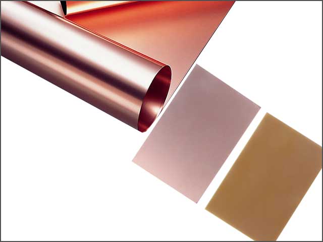
4. Copper Clad
What hasn’t been saying about a copper-clad PCB? You need to ask an Engineer and watch him go on and on about the undeniable yet equally essential advantages, along with being economically cheap; the copper clad is the board most engineers choose when creating a PCB.
The copper-clad PCB gives you the ease of soldering components over the circuit because it is created; it is excellent for designing courses.
The competitive nature of the material for Copper clad PCB makes it easy to customize the size and shape of the board compared to other boards. Due to their materials available, it causes a drop in electronic devices compared to the cost of other PCB.
Out of numerous applications of the copper-clad PCBs, some of them have been mentioned. Copper-clad PCBs are commonly used in weapons control systems, the power supplied for radar systems, primary and secondary windings of high power planar transformers, power distribution panels, and battery charger and monitoring systems.
4.1 Copper PCB—Copper Clad Laminate:
It is abbreviated as CCL(Copper Clad Laminate) and refers to a base material made of wood pulp paper or glass fibers soaked in resin and reinforcement material.
CCL can be categorized as:
- 1.CCL based on mechanical rigidity – this type of CCL are rigid
- 2.CCL based on insulation with an organic resin.
- 3.CCL based on thickness it usually is about 0.55 mm
- 4.Insulation resin CCL.
There are different types of CCL
They are classified according to different classification standards, either based on Mechanical Rigidity, Insulation Material, thickness, and Reinforcing material types.
- 1.By Mechanical Rigidity: You have a rigid CCL (G10, FR-4, CEM -1) and flex CCL, rigid PCB depends on rigid CCL while flex PCB depends on flex CCL.
- 2.By Insulation Material: You have organic resin CCL, metal base CCL, Ceramic base CCL as well as many others
- 3.By Thickness: You have your standard thick CCL and your thin CCL, for the thick CCL we have a required > 0.5mm thickness, and for the thin CCL, we have a required < 0.5mm thickness
- 4.By Reinforced Material: we have the glass fiber base (FR -4), the paper base (XPC), compound CCL (CEM -1, CEM -3).
- 5.By Applied Insulation Resin: We have epoxy resin CCL (FR -4, CEM -3) and phenolic CCL (FR -1, XPC).
4.2 Copper PCB—Quick Question: What Makes An Excellent CCL?
Simple, an excellent CCL needs to meet specific requirements to be called EXCELLENT, which includes
♦ Appearance:
do you like dents and scratches in your car? Guessing no, well same for CCL; a cut, gash, wrinkle, or pinholes can lead to low performance in the CCL and turn the PCB. So the smoother and cleaner the job, the better the performance.
♦ Size:
Your CCL is a base material for the PCB; it needs to conform to the size requirement of the PCB.
♦ Electrical Performance:
this is the primary mission of the CCL which means it’s the primary mission of the PCB; specific details have to be paid to the Volume Resistance, Insulation Resistance, Dielectric constant, Arc resistance, and so on.
♦ Physical Performance:
In physical performance, it’s always noteworthy to consider the bending strength, thermal stress, heat resistance, and punching quality.
♦ Chemical Performance:
The requirements needed to be met by the CCL are flammability, dimension stability.
♦ Environment Performance:
The CCL should meet water absorption standards.
Within the CCL is what we call a prepreg, which is reinforced material; it is the reinforcement material used in a CCL. It is made of fiber and is referred to as the bonding sheet. It is mainly made of fiber cloth, epoxy resin, acetone, and many others.
Using quality prepreg results in high-quality CCLs, which enhances the quality of PCB. The quality of the prepreg material used depends on the resin content, resin fluidity, and dicyandiamide crystallization. Consequently, you should select resin based on the quality and the cost.
The cost should be related to the thickness of the fiber cloth. Thinner prepreg is recommended even though it might be a little bit costly.
To meet Restriction of Hazardous Substances Regulations, it is recommended that you look at the reliability and heat resistance of the CCls. The latest CCL has been enhanced by modifying them so that they:
Include Halogen-free CCL – refers to CCL with the content of bromine and chlorine controlled within 900ppm. Care should be taken so that the content does not exceed 1500ppm.
Lead-free CCL – refers to Copper laminate with surface mounting that has been carried out without applying lead-free solder. The epoxy resin may be used, but the RoHS regulations must be adhered to. Note that RoHS prohibits the use of substances such as PBDE and PBBD substances.
4.3 Classification Of Resin
Resins used in CCls could be classified as:
- Epoxy resin
- Phenolic resin
- Polyamide resin
- Bismaleimide triazine
- Phenolic resin
If you are using fiber, the following quality aspects should be considered:
- Humidity resistance
- Intensity
- Insulation capability
- Heat and fire resistance
4.4 Copper PCB—Copper Laminates
This is the used clad that is over the dielectric layer and substrate (resin composite material).
The copper acts as a composite insulator material while being a good conductor, also remember. You can have rigid or flexible base material. Still, the primary purpose of the copper laminate is to act as mechanical support for the pin, i.e., the firm base that holds the electronic component and joins them at the same time.
The most popular types of copper laminates used for PCB are:
♦Polyimide:
This is a base material used for high-temperature PCB applications; it has an excellent glass transition (Tg = 220 °C) that gives it an outstanding performance over high temperatures. It allows for soldering and desoldering of components, giving you more legroom for mistakes.
♦Phenolic:
This base material is used in low-cost applications with the FR-2, CEM-1, or CEM-3 brand names. It is most widely used in single-layer PCB of small household gadgets and appliances. It is slightly brittle but hard to bend.
♦Arlon:
So far, it’s one of the most devise base materials with different applications just behind the FR -4; it is the preferred base material for multilayer PCBs; you find them in military, wireless, and communication systems.
♦FR-4:
This is a glass fiber base material that is durable, hard to bend, and cut with fire retardant qualities; it’s Tg =160°C. Because of all these qualities, various applications within single, double, and multilayer PCBs are used for power supply, mixed-signal and digital applications.
Other Copper Laminates used are Tetrafunctional epoxy, Thermount, and cyanate ester.
For electrically interconnecting the components, the laminates can be nickel, stainless steel, aluminum, and copper. However, the most widely used material for lamination purposes is copper. The aluminum found commercial applications recently and is appreciated in low-cost home appliances.
The conductive cladding layer is skinny and is over one or both sides of the resin composite material. The thickness of the cladding material is determined by how much material is deposited regarding weight.
It is a simple process but requires that you take some precautions. First, you need to turn the laminator on before feeding the board and the film in the machine. The side with the excess border should be provided into the laminator.
In most cases, you are required to put the board into the machine for the second time if you want to improve the quality of your clad board. It means that the board should be put back into the laminator immediately after it finishes the first run.
The same procedure should be used if you are working on a double-sided board.
5. Copper PCB—Copper Layer Design
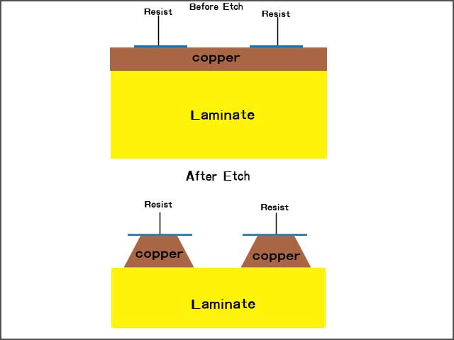
A keen eye is kept by designers when designing copper PCB; a designer must think in reverse. A board starts as solid copper; then, you remove the bits you don’t want.
It is faster to build, less expensive, and consuming when the copper is the same size as the board. Some techniques can make much difference from a frustrating experience to a smooth experience.
Maximizing copper is most common in two ways:
• Manually:
By specifying the specs of your PCBs (shape and size), this method is faster but sloppy as copper can be placed as an object, and these objects are checked for minor errors when assigned to a net. This method is mainly used for quick turns or prototype builds.
• Automatically:
However, this method is more time-consuming than the manual process, but the pour method helps to maximize copper. Copper will be left behind by drawing a border around the board area and pouring the copper in, laying out the board, and going back and placing copper shapes to fill it.
What you need to know is that when the copper pour is used, you define your boundary and everything inside when the pour operation is performed while connected automatically.
This method usually favors a large area, several irregularly shaped objects, or unusual shapes. The pour operation automatically fills the unique body while additionally isolating other traces in the area.
Objects that the copper pour can automatically handle are Traces, nets, decals, and pads. When used right, you don’t need much; the copper pouring will make the right moves and connections; you can double-check using the continuity check tool.
Now we have talked about both the manual and automatic methods, and you probably think the manual process is the best, especially for the short time sprint. Still, in the long run, the intuitive approach can be better even though it is works upfront.
There are three situations when using a copper pour might be the better option for your design.
1. Polygon Management
Manual – when you’re dealing with regular polygons, this method could be time-consuming and messy. A quick fix would be to drop overlapping shapes on top of each other to build your required profile.
It is quick, but it’s a short-term solution as eventually, you will need to do vertex editing to clean the design.
Automatic – The copper pouring method here is a “no-brainer” because we deal with complex shapes; this process is automatic. By defining the border and running copper, you eliminate the tedious job of re-editing later.
2. Plane Management
Manual – A plane is a large area of copper where all connections are one net. If you intend to build a board with separate planes while changing parts often, you often recommend route traces point to point.
Automatic – An excellent way to avoid several traces that all go to the same point is to use a copper pour method design on a plane for the ground. This will automatically connect all the connections on one network.
3. Thermal Management
Manual – if you have a Hot board with much space, the best way to cool it down is to add a copper square to help conduct the heat away. Which may not always be the case?
Automatic – when you define the area around the critical parts of the board, prioritizing them, you can minimize the thermal stress. This method is used when importance is placed on maximizing the copper surface area.
6. PCB Copper Plating And Cleaning
6.1 Copper PCB—Plating
Plating is very important to a PCB board. If all the traces on the external layers are not protected, the copper PCB will oxidize and deteriorate, making the board unstable. How do you know your copper has corroded? It will turn green. The two main reasons for plating are also called copper coating and surface finish:
1. To protect exposed copper circuitry
2. To provide a surface good enough for soldering when assembling components to the PCB.
You have various PCB copper plating options to choose from, and each carries its advantages and disadvantages. You can find them here.
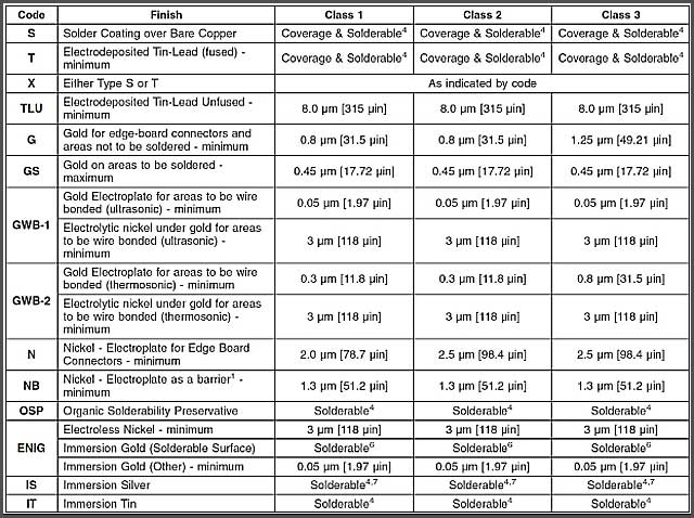
There are IPC standards for surface plating which is shown below:
6.2 Copper PCB—Clad Board Cleaning
Getting the best results is essential for you to clean your board using fine wool. You may also choose to use an abrasive pad before rinsing it with water. It helps to remove the dirt and any other contamination.
Alternatively, you may start by cleaning the dry board by exposing it to heat for about 5 minutes. This way, it ensures that the board is clean and ready for the film.
Conclusion
But I can answer you with one sentence “Copper PCB is the most reliable, effective PCB used across the most electronic device,” you don’t need to take my word for it. Just take a look at your phones.
And we at WellPCB are here to meet your needs at any time.


