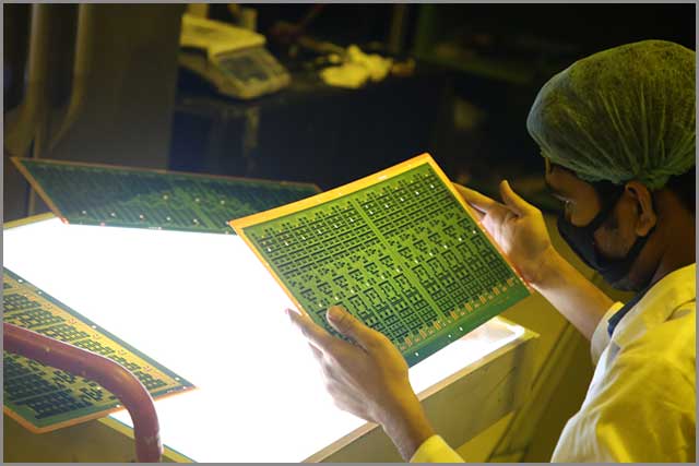
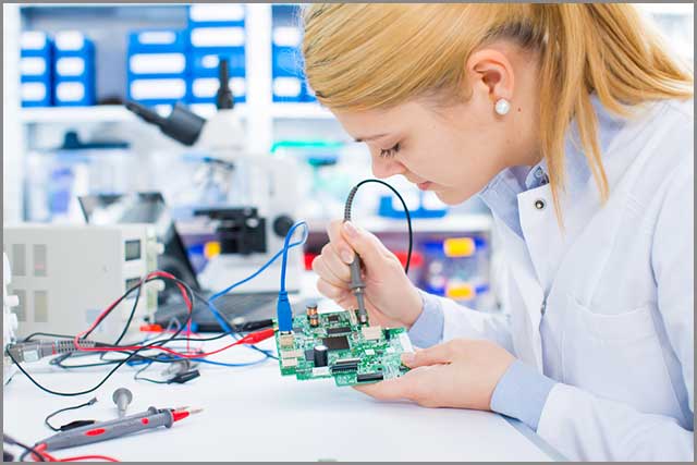
PCB manufacturing involves many processes. Manufacturers often use unique procedures to enhance the quality and efficiency of their PCBs. Any designer, engineer, or manufacturer needs to be aware of these individual processes. Only then can they select the right method for ensuring project success.
Today we will take a look at individual processes in printed circuit board manufacturing. We want to make you aware so that you can choose the right method for maximum efficiency. So, determine your project requirements and select the processes that apply to your case.
Contents
- 1 How to Identify the Special Size of the PCB
- 2 Several Types of Special PCB Materials
- 3 In the PCB Assembly Special Solder Mask and Silkscreen
- 4 PCB Manufacturing–Drills or Vias
- 5 PCB Manufacturing–Important Surface Treatment for PCB Assembly
- 6 PCB Manufacturing– Electrical Testing-Important Steps to Detect the Function of the PCB
- 7 PCB Manufacturing– Precautions
- 8 PCB Manufacturing–Conclusion
How to Identify the Special Size of the PCB
You can have PCBs of any shape or size based on your application. Let’s see the unique shapes and sizes that you can use for your PCB project.
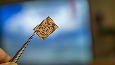
Special PCB Shapes
We see PCBs often coming in square or rectangle shapes. But you can make PCBs of any kind, such as:
- Round
- “L” shaped
- Polygon
- Oval
Indeed, there’s no end to ways you can give to your PCB. The different ways fulfill different purposes and fit in various enclosures.
You can use your PCB design tool to create PCBs of various shapes. Use the PCB editing window and choose a new design based on how you want to use it. You can also create your form or edit current ones using the editor.
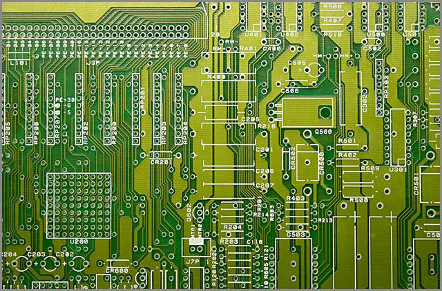
PCB Manufacturing–Special PCB Sizes
Just like PCB shapes, PCB sizes can also vary. Here we are talking about PCB panel sizes. The standard PCB size for most manufacturers is 18 x 24 inches. You can also have other formats like 12 x 18 inches, 21 x 29 inches, and so on.
You should choose a size that is suitable for your application.
Now we will explore different PCB materials.
Several Types of Special PCB Materials
You can make PCBs from a range of materials like epoxy, Teflon, and metal. Some of the unique materials include-
TG 150
TG refers to the glass transition temperature. The value refers to the heat resistance of PCB material. The higher the TG, the more is the heat resistance. TG 150 is a high heat-resistant material that you make from flame-retardant fiberglass reinforced epoxy. They are also known as FR-4 and can withstand high temperatures.
PCB Manufacturing–TG 170
TG 170 has a higher heat resistance than TG 150. You can use the material for high-temperature electronic applications. The content will withstand heat effectively and change to liquid over temperatures of 170-degree C.
Rogers PCB
Rogers is a PCB manufacturing company specializing in high-frequency PCBs. The Rogers PCBs use FR-4 laminates and use Teflon for higher-frequency properties. They can be expensive than fiberglass but is resistant to losses in higher frequencies.
You should select material based on your project requirements.
In the next chapter, we will take a look at solder mask options.
In the PCB Assembly Special Solder Mask and Silkscreen
A solder mask is a permanent layer that you apply to PCBs. Solder mask safeguards copper traces and interfaces in the board. The coating prevents conductive solder bridging and eliminates short circuits.
What is Liquid Ink Photoimageable Solder Mask?
Liquid Ink Photoimageable or LPI solder mask is an ink formula. You can spray LPI on PCBs and expose them to UV light to develop desired patterns.
What is Dry Film Photoimageable Solder Mask?
It would help if ydAfter development, you can solder parts on copper pads using the openings in the pattern. It would help if you used a vacuum to apply a Dry Film photo imageable solder mask. Then you have the copper layer on the board, which you send for thermal curing.
What is Epoxy Liquid Solder Mask?
The epoxy liquid is the cheapest solder mask, and you apply it on PCB through silkscreen. Epoxy is a thermosetting polymer, and you use them for various electronic applications.
PCB Manufacturing–What is Silkscreen?
The silkscreen is the markings or letters that you use to identify PCB components and parts. Silkscreen uses inks of different colors like white, red, black, or yellow. You can apply silkscreen using three processes-
- Manual screen-printing
- LPI (Liquid Photo Imaging)
- DLP (Direct Legend Printing)
Now comes the turn to explore PCB vias and drills.
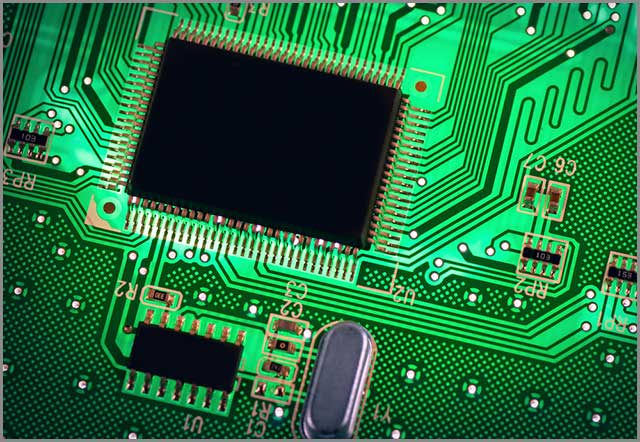
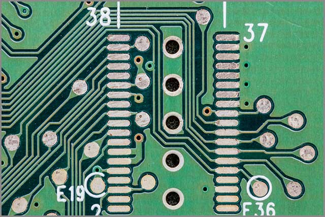
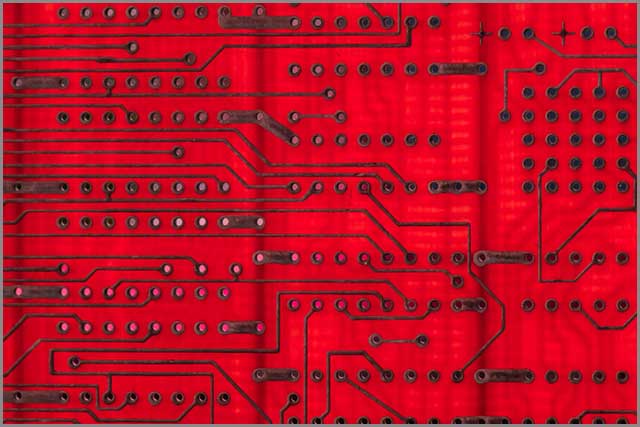
PCB Manufacturing–Drills or Vias
Vias offers a conductive path for carrying an electrical signal in a PCB. Vias use plating holes to do their job and can be of different types. Here’s a breakdown of the special via processes-
Back drill/counterbore: Counterbore holes are standard screw holes drilled on the PCB. They can fit regular socket cap screws. Back drills negate transmission and connection to prevent reflection and scattering.
Plugged vias: You can fill vias using a mask or other non-conductive material. Before applying the cap, the hole is plated with copper.
Buried and blind vias: You use a blind via to connect inner layers with one outer layer. It doesn’t penetrate the whole board.
Buried vias connect at least two inner layers but are invisible from the outside. Both processes are ideal for space-restricted PCBs.
Inner hole: Inner hole is a type of process to make multi-layer PCBs.
Micro via: Micro vias is tiny holes drilled by a laser on a PCB. They create electrical connections in a multi-layer PCB.
Tenting vias: You can use Vias to the tent and cover the hole and annular ring with a solder mask. The process reduces the number of conductive pads that you can see otherwise.
Milling blind shot: Milling refers to removing copper from the board to create a PCB according to the layout. It is a chemical-free process, unlike etching.

PCB Manufacturing–Important Surface Treatment for PCB Assembly
You often find a surface finish on PCBs for protection and optimum solderability. Some of the joint surface finishes include-
Hard Gold
and gold is a suitable finish for keypads and edge connector fingers. Hard gold is very durable but is also expensive. It comes with a layer of gold that you apply over a barrier coat of nickel. The solid gold finish is labor-intensive and needs extra processing.
PCB Manufacturing–Nickel Palladium
Nickel palladium finish is that you apply on PCB to make it resistant to abrasion. The process also improves conductivity and protects the copper layers. It is a simple process but not suitable for PCBs with higher density.
Immersion Tin/Silver/Gold
You can also use immersion tin, silver, and gold for the PCB surface finish. Immersion silver is ideal for fine traces and follows a simple finishing process. But it is difficult to electric test and may have welding durability issues.
You use immersion tin for lead-free soldering and is suitable for SMT. But the material needs careful storage and is not ideal for contact switches.
Immersion gold or ENIG is a standard surface finish and provides a flat surface for SMT. You can also use it for through-hole and high thick panels. Immersion gold has a higher resistance to environmental attacks.
PCB Manufacturing–Gold Fingers
PCB connection points have to endure continuous plugging and unplugging. As a result, they can be vulnerable to malfunctioning. Connectors are plated with gold or other metals to strengthen edge connectors. It makes them endure wear and tear effectively.
Now let’s check out the tooling implications for PCBs.
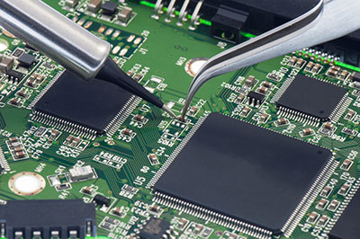
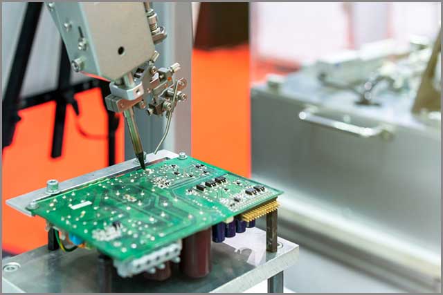
PCB Manufacturing– Electrical Testing-Important Steps to Detect the Function of the PCB
After the surface treatment, we need to detect the function of the PCB. Engineers perform mainly two types of tests- circuit continuity and isolation checks.
You will need to test the board to ensure there are no open circuits or short circuits. Electrical testing also determines the integrity of through-hole interconnections and tracks.
Sometimes, you also use the flying probe testing. The process uses moving probes to check the electrical performance of each net on a bare PCB. It would help if you had electrical testing to ensure the quality and performance of your PCB batch.
PCB Manufacturing– Precautions
PCB Manufacturing–Tooling
Tooling is the process of creating PCBA; it’s the programming that you use to control pick and place mounting. You do tooling only once for a project, and you do not need any repeat order.
Halogen Free
Some PCB materials that fall under the family of Halogen elements can be toxic and harmful to humans. Some halogen elements include-
- Bromine
- Fluorine
- Iodine
- Chlorine
- Astatine
Halogen-free PCBs have deficient levels of halogens to promote safety and health.
PCB Manufacturing–HF / CIT
You use the CIT technology to print copper on flexible substrates like PET. It is a low-cost process idea for rapid prototyping.
HF or high-frequency PCB is typically made of PTFE material. They are suitable for high-frequency applications over 1 GHz.
Now let’s check out the PCB electrical testing process.
PCB Manufacturing–Conclusion
WellPCB. We will provide you with a one-stop service and high-quality products. You can send us the documents you need to make and get a quote immediately! What are we waiting for? We have ten years of PCB manufacturing uses unique processes to suit your needs. It would help if you chose a suitable means to derive maximum efficiency and functionality. We can manufacture PCBs using the right methods so that your project is profitable. Get in touch with us to know more about our PCB processes.